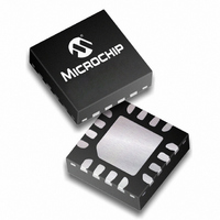
PIC16F688-E/ML Microchip Technology, PIC16F688-E/ML Datasheet - Page 73

PIC16F688-E/ML
Manufacturer Part Number
PIC16F688-E/ML
Description
IC PIC MCU FLASH 4KX14 16QFN
Manufacturer
Microchip Technology
Series
PIC® 16Fr
Datasheets
1.PIC16F616T-ISL.pdf
(8 pages)
2.PIC16F688T-ISL.pdf
(204 pages)
3.PIC16F688T-ISL.pdf
(6 pages)
4.PIC16F688T-ISL.pdf
(4 pages)
5.PIC16F688T-ISL.pdf
(688 pages)
Specifications of PIC16F688-E/ML
Core Size
8-Bit
Program Memory Size
7KB (4K x 14)
Core Processor
PIC
Speed
20MHz
Connectivity
UART/USART
Peripherals
Brown-out Detect/Reset, POR, WDT
Number Of I /o
12
Program Memory Type
FLASH
Eeprom Size
256 x 8
Ram Size
256 x 8
Voltage - Supply (vcc/vdd)
2 V ~ 5.5 V
Data Converters
A/D 8x10b
Oscillator Type
Internal
Operating Temperature
-40°C ~ 125°C
Package / Case
16-QFN
Controller Family/series
PIC16F
No. Of I/o's
12
Eeprom Memory Size
256Byte
Ram Memory Size
256Byte
Cpu Speed
20MHz
No. Of Timers
2
Processor Series
PIC16F
Core
PIC
Data Bus Width
8 bit
Data Ram Size
256 B
Interface Type
EUSART, RS- 232, SCI, USB
Maximum Clock Frequency
20 MHz
Number Of Programmable I/os
12
Number Of Timers
2
Maximum Operating Temperature
+ 125 C
Mounting Style
SMD/SMT
3rd Party Development Tools
52715-96, 52716-328, 52717-734
Development Tools By Supplier
PG164130, DV164035, DV244005, DV164005, PG164120, ICE2000, DM163014, DM164120-4
Minimum Operating Temperature
- 40 C
On-chip Adc
10 bit, 8 Channel
Lead Free Status / RoHS Status
Lead free / RoHS Compliant
For Use With
AC164324 - MODULE SKT FOR MPLAB 8DFN/16QFNXLT16QFN1 - SOCKET TRANSITION 14DIP TO 16QFNAC162061 - HEADER INTRFC MPLAB ICD2 20PINAC162056 - HEADER INTERFACE ICD2 16F688
Lead Free Status / Rohs Status
Details
- PIC16F616T-ISL PDF datasheet
- PIC16F688T-ISL PDF datasheet #2
- PIC16F688T-ISL PDF datasheet #3
- PIC16F688T-ISL PDF datasheet #4
- PIC16F688T-ISL PDF datasheet #5
- Current page: 73 of 688
- Download datasheet (3Mb)
4.2
1997 Microchip Technology Inc.
OSC2/CLKOUT
(RC mode)
Clocking Scheme/Instruction Cycle
OSC1
Q4
PC
Q2
Q3
Q1
The clock input (from OSC1) is internally divided by four to generate four non-overlapping
quadrature clocks, namely Q1, Q2, Q3, and Q4. Internally, the program counter (PC) is incre-
mented every Q1, and the instruction is fetched from the program memory and latched into the
instruction register in Q4. The instruction is decoded and executed during the following Q1
through Q4. The clocks and instruction execution flow are illustrated in
Example
Figure 4-3: Clock/Instruction Cycle
Q1
Execute INST (PC-1)
Fetch INST (PC)
Q2
T
4-1.
CY
PC
1
Q3
Q4
Q1
Execute INST (PC)
Fetch INST (PC+1)
Section 4. Architecture
Q2
T
PC+1
CY
2
Q3
Q4
Q1
Execute INST (PC+1)
Fetch INST (PC+2)
Q2
T
PC+2
CY
3
Q3
Q4
DS31004A-page 4-5
Figure
Internal
phase
clock
4-3, and
4
Related parts for PIC16F688-E/ML
Image
Part Number
Description
Manufacturer
Datasheet
Request
R

Part Number:
Description:
Manufacturer:
Microchip Technology Inc.
Datasheet:

Part Number:
Description:
IC PIC MCU FLASH 4KX14 14SOIC
Manufacturer:
Microchip Technology
Datasheet:

Part Number:
Description:
IC MCU FLASH 4KX14 14TSSOP
Manufacturer:
Microchip Technology
Datasheet:

Part Number:
Description:
IC PIC MCU FLASH 4KX14 14DIP
Manufacturer:
Microchip Technology
Datasheet:

Part Number:
Description:
IC PIC MCU FLASH 4KX14 16QFN
Manufacturer:
Microchip Technology
Datasheet:

Part Number:
Description:
IC MCU PIC FLASH 4KX14 14SOIC
Manufacturer:
Microchip Technology
Datasheet:

Part Number:
Description:
IC PIC MCU FLASH 4KX14 14TSSOP
Manufacturer:
Microchip Technology
Datasheet:

Part Number:
Description:
IC MCU PIC FLASH 4KX14 14DIP
Manufacturer:
Microchip Technology
Datasheet:

Part Number:
Description:
IC PIC MCU FLASH 4KX14 14TSSOP
Manufacturer:
Microchip Technology
Datasheet:

Part Number:
Description:
IC, 8BIT MCU, PIC16F, 32MHZ, SOIC-18
Manufacturer:
Microchip Technology
Datasheet:

Part Number:
Description:
IC, 8BIT MCU, PIC16F, 32MHZ, SSOP-20
Manufacturer:
Microchip Technology
Datasheet:

Part Number:
Description:
IC, 8BIT MCU, PIC16F, 32MHZ, DIP-18
Manufacturer:
Microchip Technology
Datasheet:

Part Number:
Description:
IC, 8BIT MCU, PIC16F, 32MHZ, QFN-28
Manufacturer:
Microchip Technology
Datasheet:

Part Number:
Description:
IC, 8BIT MCU, PIC16F, 32MHZ, QFN-28
Manufacturer:
Microchip Technology
Datasheet:

Part Number:
Description:
IC, 8BIT MCU, PIC16F, 32MHZ, QFN-28
Manufacturer:
Microchip Technology
Datasheet:


