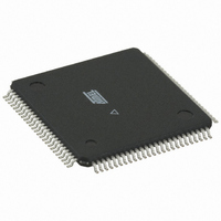
ATMEGA3290PV-10AUR Atmel, ATMEGA3290PV-10AUR Datasheet - Page 152

ATMEGA3290PV-10AUR
Manufacturer Part Number
ATMEGA3290PV-10AUR
Description
MCU AVR 32K FLASH 10MHZ 64TQFP
Manufacturer
Atmel
Series
AVR® ATmegar
Specifications of ATMEGA3290PV-10AUR
Core Processor
AVR
Core Size
8-Bit
Speed
10MHz
Connectivity
SPI, UART/USART, USI
Peripherals
Brown-out Detect/Reset, LCD, POR, PWM, WDT
Number Of I /o
69
Program Memory Size
32KB (16K x 16)
Program Memory Type
FLASH
Eeprom Size
1K x 8
Ram Size
2K x 8
Voltage - Supply (vcc/vdd)
1.8 V ~ 5.5 V
Data Converters
A/D 8x10b
Oscillator Type
Internal
Operating Temperature
-40°C ~ 85°C
Package / Case
*
Lead Free Status / RoHS Status
Lead free / RoHS Compliant
Available stocks
Company
Part Number
Manufacturer
Quantity
Price
- Current page: 152 of 427
- Download datasheet (9Mb)
17.9
8021G–AVR–03/11
Asynchronous Operation of Timer/Counter2
Figure 17-11. Timer/Counter Timing Diagram, Clear Timer on Compare Match mode, with Pres-
When Timer/Counter2 operates asynchronously, some considerations must be taken.
• Warning: When switching between asynchronous and synchronous clocking of
1. Disable the Timer/Counter2 interrupts by clearing OCIE2A and TOIE2.
2. Select clock source by setting AS2 as appropriate.
3. Write new values to TCNT2, OCR2A, and TCCR2A.
4. To switch to asynchronous operation: Wait for TCN2UB, OCR2UB, and TCR2UB.
5. Clear the Timer/Counter2 Interrupt Flags.
6. Enable interrupts, if needed.
• The CPU main clock frequency must be more than four times the Oscillator frequency.
• When writing to one of the registers TCNT2, OCR2A, or TCCR2A, the value is transferred to a
• When entering Power-save or ADC Noise Reduction mode after having written to TCNT2,
• If Timer/Counter2 is used to wake the device up from Power-save or ADC Noise Reduction
Timer/Counter2, the Timer Registers TCNT2, OCR2A, and TCCR2A might be corrupted. A
safe procedure for switching clock source is:
temporary register, and latched after two positive edges on TOSC1. The user should not write
a new value before the contents of the temporary register have been transferred to its
destination. Each of the three mentioned registers have their individual temporary register,
which means that e.g. writing to TCNT2 does not disturb an OCR2A write in progress. To
detect that a transfer to the destination register has taken place, the Asynchronous Status
Register – ASSR has been implemented.
OCR2A, or TCCR2A, the user must wait until the written register has been updated if
Timer/Counter2 is used to wake up the device. Otherwise, the MCU will enter sleep mode
before the changes are effective. This is particularly important if the Output Compare2 interrupt
is used to wake up the device, since the Output Compare function is disabled during writing to
OCR2A or TCNT2. If the write cycle is not finished, and the MCU enters sleep mode before the
OCR2UB bit returns to zero, the device will never receive a compare match interrupt, and the
MCU will not wake up.
mode, precautions must be taken if the user wants to re-enter one of these modes: The
interrupt logic needs one TOSC1 cycle to be reset. If the time between wake-up and reentering
sleep mode is less than one TOSC1 cycle, correct interrupt handling is not guaranteed. If the
TCNTn
(clk
OCRnx
(CTC)
OCFnx
clk
clk
I/O
I/O
Tn
/8)
caler (f
clk_I/O
TOP - 1
/8)
TOP
TOP
ATmega329P/3290P
BOTTOM
BOTTOM + 1
152
Related parts for ATMEGA3290PV-10AUR
Image
Part Number
Description
Manufacturer
Datasheet
Request
R

Part Number:
Description:
IC MCU 32K 4X40 LCD CTRL 100TQFP
Manufacturer:
Atmel
Datasheet:

Part Number:
Description:
Manufacturer:
Atmel Corporation
Datasheet:

Part Number:
Description:
MCU AVR 32K FLASH 20MHZ 64TQFP
Manufacturer:
Atmel
Datasheet:

Part Number:
Description:
Manufacturer:
Atmel Corporation
Datasheet:

Part Number:
Description:
IC AVR MCU 32K 16MHZ 100TQFP
Manufacturer:
Atmel
Datasheet:

Part Number:
Description:
IC AVR MCU 32K 16MHZ 100TQFP
Manufacturer:
Atmel
Datasheet:

Part Number:
Description:
MCU AVR 32K FLASH 16MHZ 64TQFP
Manufacturer:
Atmel
Datasheet:

Part Number:
Description:
Atmega3290 Avr 8-bit Microcontroller With In-system Programmable Flash
Manufacturer:
ATMEL Corporation
Datasheet:

Part Number:
Description:
IC AVR MCU 32K 16MHZ 5V 44-QFN
Manufacturer:
Atmel
Datasheet:

Part Number:
Description:
IC AVR MCU 32K 16MHZ 5V 40DIP
Manufacturer:
Atmel
Datasheet:

Part Number:
Description:
IC AVR MCU 32K 16MHZ 5V 44TQFP
Manufacturer:
Atmel
Datasheet:

Part Number:
Description:
IC AVR MCU 32K 16MHZ IND 40-DIP
Manufacturer:
Atmel
Datasheet:

Part Number:
Description:
IC AVR MCU 32K 16MHZ IND 44-TQFP
Manufacturer:
Atmel
Datasheet:

Part Number:
Description:
Manufacturer:
Atmel Corporation
Datasheet:


