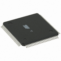
ATMEGA3290PV-10AUR Atmel, ATMEGA3290PV-10AUR Datasheet - Page 256

ATMEGA3290PV-10AUR
Manufacturer Part Number
ATMEGA3290PV-10AUR
Description
MCU AVR 32K FLASH 10MHZ 64TQFP
Manufacturer
Atmel
Series
AVR® ATmegar
Specifications of ATMEGA3290PV-10AUR
Core Processor
AVR
Core Size
8-Bit
Speed
10MHz
Connectivity
SPI, UART/USART, USI
Peripherals
Brown-out Detect/Reset, LCD, POR, PWM, WDT
Number Of I /o
69
Program Memory Size
32KB (16K x 16)
Program Memory Type
FLASH
Eeprom Size
1K x 8
Ram Size
2K x 8
Voltage - Supply (vcc/vdd)
1.8 V ~ 5.5 V
Data Converters
A/D 8x10b
Oscillator Type
Internal
Operating Temperature
-40°C ~ 85°C
Package / Case
*
Lead Free Status / RoHS Status
Lead free / RoHS Compliant
Available stocks
Company
Part Number
Manufacturer
Quantity
Price
- Current page: 256 of 427
- Download datasheet (9Mb)
25.3.4
25.4
25.4.1
25.4.2
8021G–AVR–03/11
Boundary-scan Specific JTAG Instructions
Boundary-scan Chain
EXTEST; 0x0
IDCODE; 0x1
Figure 25-1. Reset Register
The Boundary-scan Chain has the capability of driving and observing the logic levels on the dig-
ital I/O pins, as well as the boundary between digital and analog logic for analog circuitry having
off-chip connections.
See
The Instruction Register is 4-bit wide, supporting up to 16 instructions. Listed below are the
JTAG instructions useful for Boundary-scan operation. Note that the optional HIGHZ instruction
is not implemented, but all outputs with tri-state capability can be set in high-impedant state by
using the AVR_RESET instruction, since the initial state for all port pins is tri-state.
As a definition in this data sheet, the LSB is shifted in and out first for all Shift Registers.
The OPCODE for each instruction is shown behind the instruction name in hex format. The text
describes which Data Register is selected as path between TDI and TDO for each instruction.
Mandatory JTAG instruction for selecting the Boundary-scan Chain as Data Register for testing
circuitry external to the AVR package. For port-pins, Pull-up Disable, Output Control, Output
Data, and Input Data are all accessible in the scan chain. For Analog circuits having off-chip
connections, the interface between the analog and the digital logic is in the scan chain. The con-
tents of the latched outputs of the Boundary-scan chain is driven out as soon as the JTAG IR-
Register is loaded with the EXTEST instruction.
The active states are:
• Capture-DR: Data on the external pins are sampled into the Boundary-scan Chain.
• Shift-DR: The Internal Scan Chain is shifted by the TCK input.
• Update-DR: Data from the scan chain is applied to output pins.
Optional JTAG instruction selecting the 32 bit ID-Register as Data Register. The ID-Register
consists of a version number, a device number and the manufacturer code chosen by JEDEC.
This is the default instruction after power-up.
”Boundary-scan Chain” on page 257
From Other Internal and
External Reset Sources
From
ClockDR · AVR_RESET
TDI
D
for a complete description.
Q
TDO
To
ATmega329P/3290P
Internal reset
256
Related parts for ATMEGA3290PV-10AUR
Image
Part Number
Description
Manufacturer
Datasheet
Request
R

Part Number:
Description:
IC MCU 32K 4X40 LCD CTRL 100TQFP
Manufacturer:
Atmel
Datasheet:

Part Number:
Description:
Manufacturer:
Atmel Corporation
Datasheet:

Part Number:
Description:
MCU AVR 32K FLASH 20MHZ 64TQFP
Manufacturer:
Atmel
Datasheet:

Part Number:
Description:
Manufacturer:
Atmel Corporation
Datasheet:

Part Number:
Description:
IC AVR MCU 32K 16MHZ 100TQFP
Manufacturer:
Atmel
Datasheet:

Part Number:
Description:
IC AVR MCU 32K 16MHZ 100TQFP
Manufacturer:
Atmel
Datasheet:

Part Number:
Description:
MCU AVR 32K FLASH 16MHZ 64TQFP
Manufacturer:
Atmel
Datasheet:

Part Number:
Description:
Atmega3290 Avr 8-bit Microcontroller With In-system Programmable Flash
Manufacturer:
ATMEL Corporation
Datasheet:

Part Number:
Description:
IC AVR MCU 32K 16MHZ 5V 44-QFN
Manufacturer:
Atmel
Datasheet:

Part Number:
Description:
IC AVR MCU 32K 16MHZ 5V 40DIP
Manufacturer:
Atmel
Datasheet:

Part Number:
Description:
IC AVR MCU 32K 16MHZ 5V 44TQFP
Manufacturer:
Atmel
Datasheet:

Part Number:
Description:
IC AVR MCU 32K 16MHZ IND 40-DIP
Manufacturer:
Atmel
Datasheet:

Part Number:
Description:
IC AVR MCU 32K 16MHZ IND 44-TQFP
Manufacturer:
Atmel
Datasheet:

Part Number:
Description:
Manufacturer:
Atmel Corporation
Datasheet:


