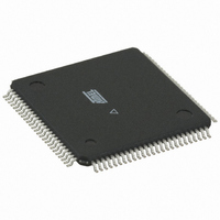
ATMEGA3290PV-10AUR Atmel, ATMEGA3290PV-10AUR Datasheet - Page 242

ATMEGA3290PV-10AUR
Manufacturer Part Number
ATMEGA3290PV-10AUR
Description
MCU AVR 32K FLASH 10MHZ 64TQFP
Manufacturer
Atmel
Series
AVR® ATmegar
Specifications of ATMEGA3290PV-10AUR
Core Processor
AVR
Core Size
8-Bit
Speed
10MHz
Connectivity
SPI, UART/USART, USI
Peripherals
Brown-out Detect/Reset, LCD, POR, PWM, WDT
Number Of I /o
69
Program Memory Size
32KB (16K x 16)
Program Memory Type
FLASH
Eeprom Size
1K x 8
Ram Size
2K x 8
Voltage - Supply (vcc/vdd)
1.8 V ~ 5.5 V
Data Converters
A/D 8x10b
Oscillator Type
Internal
Operating Temperature
-40°C ~ 85°C
Package / Case
*
Lead Free Status / RoHS Status
Lead free / RoHS Compliant
Available stocks
Company
Part Number
Manufacturer
Quantity
Price
- Current page: 242 of 427
- Download datasheet (9Mb)
23.5.2
8021G–AVR–03/11
LCDCRB – LCD Control and Status Register B
• Bit 0 – LCDBL: LCD Blanking
When this bit is written to one, the display will be blanked after completion of a frame. All seg-
ment and common pins will be driven to ground.
Note:
• Bit 7 – LCDCS: LCD Clock Select
When this bit is written to zero, the system clock is used. When this bit is written to one, the
external asynchronous clock source is used. The asynchronous clock source is either
Timer/Counter Oscillator or external clock, depending on EXCLK in ASSR. See
Operation of Timer/Counter2” on page 152
• Bit 6 – LCD2B: LCD 1/2 Bias Select
When this bit is written to zero, 1/3 bias is used. When this bit is written to one, ½ bias is used.
Refer to the LCD Manufacture for recommended bias selection.
• Bit 5:4 – LCDMUX1:0: LCD Mux Select
The LCDMUX1:0 bits determine the duty cycle. Common pins that are not used are ordinary port
pins. The different duty selections are shown in
Table 23-2.
Note:
• Bits 3:0 – LCDPM3:0: LCD Port Mask
The LCDPM3:0 bits determine the number of port pins to be used as segment drivers. The dif-
ferent selections are shown in
Table 23-3.
Bit
(0xE5)
Read/Write
Initial Value
LCDPM3
LCDMUX1
0
0
0
0
0
0
1
1
Bit 3, LCDPM3 is only available in ATmega3290P.
1. 1/2 bias when LCD2B is written to one and 1/3 otherwise.
LCDCS
R/W
LCDPM2
LCD Duty Select
LCD Port Mask (Values in bold are only available in ATmega3290P)
7
0
LCDMUX0
0
0
0
0
0
1
0
1
LCD2B
R/W
6
0
LCDPM1
0
0
1
1
LCDMUX1
Table
R/W
5
0
Static
Duty
1/2
1/3
1/4
23-3. Unused pins can be used as ordinary port pins.
LCDPM0
LCDMUX0
0
1
0
1
R/W
for further details.
4
0
1/2 or 1/3
1/2 or 1/3
1/2 or 1/3
Table
Static
Bias
LCDPM3
R/W
I/O Port in Use as
Segment Driver
3
0
(1)
(1)
(1)
23-2.
SEG0:12
SEG0:14
SEG0:16
SEG0:18
ATmega329P/3290P
LCDPM2
COM Pin
R/W
COM0:1
COM0:2
COM0:3
COM0
2
0
LCDPM1
R/W
1
0
Maximum Number
of Segments
LCDPM0
I/O Port Pin
R/W
”Asynchronous
COM1:3
COM2:3
0
0
COM3
None
13
15
17
19
LCDCRB
242
Related parts for ATMEGA3290PV-10AUR
Image
Part Number
Description
Manufacturer
Datasheet
Request
R

Part Number:
Description:
IC MCU 32K 4X40 LCD CTRL 100TQFP
Manufacturer:
Atmel
Datasheet:

Part Number:
Description:
Manufacturer:
Atmel Corporation
Datasheet:

Part Number:
Description:
MCU AVR 32K FLASH 20MHZ 64TQFP
Manufacturer:
Atmel
Datasheet:

Part Number:
Description:
Manufacturer:
Atmel Corporation
Datasheet:

Part Number:
Description:
IC AVR MCU 32K 16MHZ 100TQFP
Manufacturer:
Atmel
Datasheet:

Part Number:
Description:
IC AVR MCU 32K 16MHZ 100TQFP
Manufacturer:
Atmel
Datasheet:

Part Number:
Description:
MCU AVR 32K FLASH 16MHZ 64TQFP
Manufacturer:
Atmel
Datasheet:

Part Number:
Description:
Atmega3290 Avr 8-bit Microcontroller With In-system Programmable Flash
Manufacturer:
ATMEL Corporation
Datasheet:

Part Number:
Description:
IC AVR MCU 32K 16MHZ 5V 44-QFN
Manufacturer:
Atmel
Datasheet:

Part Number:
Description:
IC AVR MCU 32K 16MHZ 5V 40DIP
Manufacturer:
Atmel
Datasheet:

Part Number:
Description:
IC AVR MCU 32K 16MHZ 5V 44TQFP
Manufacturer:
Atmel
Datasheet:

Part Number:
Description:
IC AVR MCU 32K 16MHZ IND 40-DIP
Manufacturer:
Atmel
Datasheet:

Part Number:
Description:
IC AVR MCU 32K 16MHZ IND 44-TQFP
Manufacturer:
Atmel
Datasheet:

Part Number:
Description:
Manufacturer:
Atmel Corporation
Datasheet:


