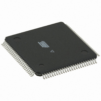
ATMEGA3290PV-10AUR Atmel, ATMEGA3290PV-10AUR Datasheet - Page 306

ATMEGA3290PV-10AUR
Manufacturer Part Number
ATMEGA3290PV-10AUR
Description
MCU AVR 32K FLASH 10MHZ 64TQFP
Manufacturer
Atmel
Series
AVR® ATmegar
Specifications of ATMEGA3290PV-10AUR
Core Processor
AVR
Core Size
8-Bit
Speed
10MHz
Connectivity
SPI, UART/USART, USI
Peripherals
Brown-out Detect/Reset, LCD, POR, PWM, WDT
Number Of I /o
69
Program Memory Size
32KB (16K x 16)
Program Memory Type
FLASH
Eeprom Size
1K x 8
Ram Size
2K x 8
Voltage - Supply (vcc/vdd)
1.8 V ~ 5.5 V
Data Converters
A/D 8x10b
Oscillator Type
Internal
Operating Temperature
-40°C ~ 85°C
Package / Case
*
Lead Free Status / RoHS Status
Lead free / RoHS Compliant
Available stocks
Company
Part Number
Manufacturer
Quantity
Price
- Current page: 306 of 427
- Download datasheet (9Mb)
27.7.5
27.7.6
8021G–AVR–03/11
Programming the EEPROM
Reading the Flash
The EEPROM is organized in pages, see
EEPROM, the program data is latched into a page buffer. This allows one page of data to be
programmed simultaneously. The programming algorithm for the EEPROM data memory is as
follows (refer to
Data loading):
1. A: Load Command “0001 0001”.
2. G: Load Address High Byte (0x00 - 0xFF).
3. B: Load Address Low Byte (0x00 - 0xFF).
4. C: Load Data (0x00 - 0xFF).
5. E: Latch data (give PAGEL a positive pulse).
K: Repeat 3 through 5 until the entire buffer is filled.
L: Program EEPROM page
1. Set BS1 to “0”.
2. Give WR a negative pulse. This starts programming of the EEPROM page. RDY/BSY
3. Wait until to RDY/BSY goes high before programming the next page (See
Figure 27-4. Programming the EEPROM Waveforms
The algorithm for reading the Flash memory is as follows (refer to
page 303
1. A: Load Command “0000 0010”.
2. G: Load Address High Byte (0x00 - 0xFF).
3. B: Load Address Low Byte (0x00 - 0xFF).
4. Set OE to “0”, and BS1 to “0”. The Flash word low byte can now be read at DATA.
5. Set BS1 to “1”. The Flash word high byte can now be read at DATA.
6. Set OE to “1”.
goes low.
signal waveforms).
RESET +12V
RDY/BSY
PAGEL
XTAL1
DATA
XA1
XA0
BS1
BS2
WR
OE
for details on Command and Address loading):
”Programming the Flash” on page 303
0x11
A
ADDR. HIGH
G
ADDR. LOW
B
DATA
C
Table 27-14 on page
XX
E
ADDR. LOW
B
for details on Command, Address and
DATA
ATmega329P/3290P
C
K
XX
E
301. When programming the
”Programming the Flash” on
L
Figure 27-4
for
306
Related parts for ATMEGA3290PV-10AUR
Image
Part Number
Description
Manufacturer
Datasheet
Request
R

Part Number:
Description:
IC MCU 32K 4X40 LCD CTRL 100TQFP
Manufacturer:
Atmel
Datasheet:

Part Number:
Description:
Manufacturer:
Atmel Corporation
Datasheet:

Part Number:
Description:
MCU AVR 32K FLASH 20MHZ 64TQFP
Manufacturer:
Atmel
Datasheet:

Part Number:
Description:
Manufacturer:
Atmel Corporation
Datasheet:

Part Number:
Description:
IC AVR MCU 32K 16MHZ 100TQFP
Manufacturer:
Atmel
Datasheet:

Part Number:
Description:
IC AVR MCU 32K 16MHZ 100TQFP
Manufacturer:
Atmel
Datasheet:

Part Number:
Description:
MCU AVR 32K FLASH 16MHZ 64TQFP
Manufacturer:
Atmel
Datasheet:

Part Number:
Description:
Atmega3290 Avr 8-bit Microcontroller With In-system Programmable Flash
Manufacturer:
ATMEL Corporation
Datasheet:

Part Number:
Description:
IC AVR MCU 32K 16MHZ 5V 44-QFN
Manufacturer:
Atmel
Datasheet:

Part Number:
Description:
IC AVR MCU 32K 16MHZ 5V 40DIP
Manufacturer:
Atmel
Datasheet:

Part Number:
Description:
IC AVR MCU 32K 16MHZ 5V 44TQFP
Manufacturer:
Atmel
Datasheet:

Part Number:
Description:
IC AVR MCU 32K 16MHZ IND 40-DIP
Manufacturer:
Atmel
Datasheet:

Part Number:
Description:
IC AVR MCU 32K 16MHZ IND 44-TQFP
Manufacturer:
Atmel
Datasheet:

Part Number:
Description:
Manufacturer:
Atmel Corporation
Datasheet:


