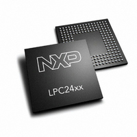
LPC2468FET208,551 NXP Semiconductors, LPC2468FET208,551 Datasheet - Page 38

LPC2468FET208,551
Manufacturer Part Number
LPC2468FET208,551
Description
IC ARM7 MCU FLASH 512K 208TFBGA
Manufacturer
NXP Semiconductors
Series
LPC2400r
Specifications of LPC2468FET208,551
Program Memory Type
FLASH
Program Memory Size
512KB (512K x 8)
Package / Case
208-TFBGA
Core Processor
ARM7
Core Size
16/32-Bit
Speed
72MHz
Connectivity
CAN, EBI/EMI, Ethernet, I²C, Microwire, MMC, SPI, SSI, SSP, UART/USART, USB OTG
Peripherals
Brown-out Detect/Reset, DMA, I²S, POR, PWM, WDT
Number Of I /o
160
Ram Size
98K x 8
Voltage - Supply (vcc/vdd)
3 V ~ 3.6 V
Data Converters
A/D 8x10b; D/A 1x10b
Oscillator Type
Internal
Operating Temperature
-40°C ~ 85°C
Processor Series
LPC24
Core
ARM7TDMI-S
Data Bus Width
16 bit, 32 bit
Data Ram Size
98 KB
Interface Type
CAN/I2S/ISP/SSP/UART/USB
Maximum Clock Frequency
72 MHz
Number Of Programmable I/os
160
Number Of Timers
6
Operating Supply Voltage
3.3 V
Maximum Operating Temperature
+ 85 C
Mounting Style
SMD/SMT
3rd Party Development Tools
MDK-ARM, RL-ARM, ULINK2, IRD-LPC2468-DEV, SAB-TFBGA208, KSK-LPC2468-PL
Development Tools By Supplier
OM10100
Minimum Operating Temperature
- 40 C
On-chip Adc
8-ch x 10-bit
On-chip Dac
1-ch x 10-bit
Package
208TFBGA
Device Core
ARM7TDMI-S
Family Name
LPC2000
Maximum Speed
72 MHz
Lead Free Status / RoHS Status
Lead free / RoHS Compliant
For Use With
622-1025 - KIT DEV IND REF DESIGN LPC2468622-1024 - BOARD SCKT ADAPTER FOR TFBGA208568-4358 - DISPLAY QVGA TFT FOR OM10100568-4309 - BOARD EXTENSION LPCSTICK568-4308 - EVAL LPC-STICK WITH LPC2468MCB2400U - BOARD EVAL MCB2400 + ULINK2MCB2400 - BOARD EVAL FOR NXP LPC246X SER622-1005 - USB IN-CIRCUIT PROG ARM7 LPC2K
Eeprom Size
-
Lead Free Status / Rohs Status
Lead free / RoHS Compliant
Other names
568-4262
935283234551
LPC2468FET208-S
935283234551
LPC2468FET208-S
Available stocks
Company
Part Number
Manufacturer
Quantity
Price
Company:
Part Number:
LPC2468FET208,551
Manufacturer:
NXP
Quantity:
6 174
Company:
Part Number:
LPC2468FET208,551
Manufacturer:
NXP Semiconductors
Quantity:
10 000
NXP Semiconductors
LPC2468
Product data sheet
7.22.1 Features
7.22 Pulse width modulator
The PWM is based on the standard Timer block and inherits all of its features, although
only the PWM function is pinned out on the LPC2468. The Timer is designed to count
cycles of the system derived clock and optionally switch pins, generate interrupts or
perform other actions when specified timer values occur, based on seven match registers.
The PWM function is in addition to these features and is based on match register events.
The ability to separately control rising and falling edge locations allows the PWM to be
used for more applications. For instance, multi-phase motor control typically requires
three non-overlapping PWM outputs with individual control of all three pulse widths and
positions.
Two match registers can be used to provide a single edge controlled PWM output. A
dedicated match register controls the PWM cycle rate, by resetting the count upon match.
The other match register controls the PWM edge position. Additional single edge
controlled PWM outputs require only one match register each, since the repetition rate is
the same for all PWM outputs. Multiple single edge controlled PWM outputs will all have a
rising edge at the beginning of each PWM cycle, when an PWMMR0 match occurs.
Three match registers can be used to provide a PWM output with both edges controlled.
Again, a dedicated match register controls the PWM cycle rate. The other match registers
control the two PWM edge positions. Additional double edge controlled PWM outputs
require only two match registers each, since the repetition rate is the same for all PWM
outputs.
With double edge controlled PWM outputs, specific match registers control the rising and
falling edge of the output. This allows both positive going PWM pulses (when the rising
edge occurs prior to the falling edge), and negative going PWM pulses (when the falling
edge occurs prior to the rising edge).
•
•
•
•
LPC2468 has two PWMs with the same operational features. These may be operated
in a synchronized fashion by setting them both up to run at the same rate, then
enabling both simultaneously. PWM0 acts as the master and PWM1 as the slave for
this use.
Counter or Timer operation (may use the peripheral clock or one of the capture inputs
as the clock source).
Seven match registers allow up to 6 single edge controlled or 3 double edge
controlled PWM outputs, or a mix of both types. The match registers also allow:
– Continuous operation with optional interrupt generation on match.
– Stop timer on match with optional interrupt generation.
– Reset timer on match with optional interrupt generation.
Supports single edge controlled and/or double edge controlled PWM outputs. Single
edge controlled PWM outputs all go HIGH at the beginning of each cycle unless the
output is a constant LOW. Double edge controlled PWM outputs can have either edge
occur at any position within a cycle. This allows for both positive going and negative
going pulses.
All information provided in this document is subject to legal disclaimers.
Rev. 5 — 15 October 2010
Single-chip 16-bit/32-bit micro
LPC2468
© NXP B.V. 2010. All rights reserved.
38 of 85


