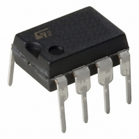
ST7FLITEU09B6 STMicroelectronics, ST7FLITEU09B6 Datasheet - Page 76

ST7FLITEU09B6
Manufacturer Part Number
ST7FLITEU09B6
Description
MCU 8BIT SGL VOLT FLASH 8-DIP
Manufacturer
STMicroelectronics
Series
ST7r
Datasheet
1.ST7FLITEU05M6.pdf
(139 pages)
Specifications of ST7FLITEU09B6
Core Processor
ST7
Core Size
8-Bit
Speed
8MHz
Peripherals
LVD, POR, PWM, WDT
Number Of I /o
5
Program Memory Size
2KB (2K x 8)
Program Memory Type
FLASH
Eeprom Size
128 x 8
Ram Size
128 x 8
Voltage - Supply (vcc/vdd)
2.4 V ~ 5.5 V
Data Converters
A/D 5x10b
Oscillator Type
Internal
Operating Temperature
-40°C ~ 85°C
Package / Case
8-DIP (0.300", 7.62mm)
Processor Series
ST7FLITEUx
Core
ST7
Data Bus Width
8 bit
Data Ram Size
128 B
Interface Type
ICC
Maximum Clock Frequency
8 MHz
Number Of Programmable I/os
5
Number Of Timers
2
Maximum Operating Temperature
+ 85 C
Mounting Style
Through Hole
Development Tools By Supplier
ST7FLITE-SK/RAIS, ST7FLITU0-D/RAIS, STX-RLINK
Minimum Operating Temperature
- 40 C
On-chip Adc
10 bit, 5 Channel
For Use With
497-5858 - EVAL BOARD PLAYBACK ST7FLITE
Lead Free Status / RoHS Status
Lead free / RoHS Compliant
Connectivity
-
Lead Free Status / Rohs Status
Details
Available stocks
Company
Part Number
Manufacturer
Quantity
Price
On-chip peripherals
Note:
Caution:
76/139
Figure 39. PWM signal example
Output compare mode
To use this function, the OE bit must be 0, otherwise the compare is done with the shadow
register instead of the DCRx register. Software must then write a 12-bit value in the DCR0H
and DCR0L registers. This value will be loaded immediately (without waiting for an OVF
event).
The DCR0H must be written first, the output compare function starts only when the DCR0L
value is written.
When the 12-bit upcounter (CNTR) reaches the value stored in the DCR0H and DCR0L
registers, the CMPF0 bit in the PWM0CSR register is set and an interrupt request is
generated if the CMPIE bit is set.
The output compare function is only available for DCRx values other than 0 (reset value).
At each OVF event, the DCRx value is written in a shadow register, even if the DCR0L value
has not yet been written (in this case, the shadow register will contain the new DCR0H value
and the old DCR0L value), then:
- If OE=1 (PWM mode): the compare is done between the timer counter and the shadow
register (and not DCRx)
- if OE=0 (OCMP mode): the compare is done between the timer counter and DCRx. There
is no PWM signal.
The compare between DCRx or the shadow register and the timer counter is locked until
DCR0L is written.
DCR0=FFEh
COUNTER
f
COUNTER
FFDh
FFEh
ATR= FFDh
FFFh
FFDh
FFEh
FFFh
ST7LITEU05 ST7LITEU09
FFDh
FFEh
t


