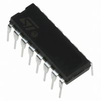
ST7FLIT10BY0B6 STMicroelectronics, ST7FLIT10BY0B6 Datasheet - Page 31

ST7FLIT10BY0B6
Manufacturer Part Number
ST7FLIT10BY0B6
Description
IC MCU 8BIT 2K FLASH 16-DIP
Manufacturer
STMicroelectronics
Series
ST7r
Datasheet
1.ST7FLIT15BY1M6.pdf
(159 pages)
Specifications of ST7FLIT10BY0B6
Core Processor
ST7
Core Size
8-Bit
Speed
8MHz
Connectivity
SPI
Peripherals
LVD, POR, PWM, WDT
Number Of I /o
11
Program Memory Size
2KB (2K x 8)
Program Memory Type
FLASH
Ram Size
256 x 8
Voltage - Supply (vcc/vdd)
2.7 V ~ 5.5 V
Data Converters
A/D 7x10b
Oscillator Type
Internal
Operating Temperature
-40°C ~ 85°C
Package / Case
16-DIP (0.300", 7.62mm)
Processor Series
ST7FLIT1x
Core
ST7
Data Bus Width
8 bit
Data Ram Size
256 B
Interface Type
SPI
Maximum Clock Frequency
8 MHz
Number Of Programmable I/os
17
Number Of Timers
4
Maximum Operating Temperature
+ 85 C
Mounting Style
Through Hole
Development Tools By Supplier
ST7FLITE-SK/RAIS, ST7MDT10-DVP3, ST7MDT10-EMU3, STX-RLINK
Minimum Operating Temperature
- 40 C
On-chip Adc
10 bit, 7 Channel
For Use With
497-5049 - KIT STARTER RAISONANCE ST7FLITE
Lead Free Status / RoHS Status
Lead free / RoHS Compliant
Eeprom Size
-
Lead Free Status / Rohs Status
Details
7.6 SYSTEM INTEGRITY MANAGEMENT (SI)
The System Integrity Management block contains
the Low voltage Detector (LVD) and Auxiliary Volt-
age Detector (AVD) functions. It is managed by
the SICSR register.
Note: A reset can also be triggered following the
detection of an illegal opcode or prebyte code. Re-
fer to
tails.
7.6.1 Low Voltage Detector (LVD)
The Low Voltage Detector function (LVD) gener-
ates a static reset when the V
below a V
it secures the power-up as well as the power-down
keeping the ST7 in reset.
The V
lower than the V
on in order to avoid a parasitic reset when the
MCU starts running and sinks current on the sup-
ply (hysteresis).
The LVD Reset circuitry generates a reset when
V
The LVD function is illustrated in
The voltage threshold can be configured by option
byte to be low, medium or high.
Figure 18. Low Voltage Detector vs Reset
DD
– V
– V
V
V
RESET
is below:
IT-
IT+
IT+(LVD)
IT-(LVD)
IT-(LVD)
section 12.2.1 on page 107
(LVD)
(LVD)
IT-(LVD)
when V
when V
reference value for a voltage drop is
V
DD
IT+(LVD)
reference value. This means that
DD
DD
reference value for power-
is rising
is falling
DD
Figure
supply voltage is
for further de-
18.
Provided the minimum V
the oscillator frequency) is above V
MCU can only be in two modes:
In these conditions, secure operation is always en-
sured for the application without the need for ex-
ternal reset hardware.
During a Low Voltage Detector Reset, the RESET
pin is held low, thus permitting the MCU to reset
other devices.
Notes:
The LVD allows the device to be used without any
external RESET circuitry.
The LVD is an optional function which can be se-
lected by option byte.
Use of LVD with capacitive power supply: with this
type of power supply, if power cuts occur in the ap-
plication, it is recommended to pull V
0V to ensure optimum restart conditions. Refer to
circuit example in
note 4.
It is recommended to make sure that the V
ply voltage rises monotonously when the device is
exiting from Reset, to ensure the application func-
tions properly.
V
– under full software control
– in static safe reset
hys
Figure 106 on page 136
DD
value (guaranteed for
ST7LITE1xB
IT-(LVD)
DD
down to
DD
31/159
, the
sup-
and
1


