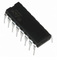
ST7FLIT10BY0B6 STMicroelectronics, ST7FLIT10BY0B6 Datasheet - Page 56

ST7FLIT10BY0B6
Manufacturer Part Number
ST7FLIT10BY0B6
Description
IC MCU 8BIT 2K FLASH 16-DIP
Manufacturer
STMicroelectronics
Series
ST7r
Datasheet
1.ST7FLIT15BY1M6.pdf
(159 pages)
Specifications of ST7FLIT10BY0B6
Core Processor
ST7
Core Size
8-Bit
Speed
8MHz
Connectivity
SPI
Peripherals
LVD, POR, PWM, WDT
Number Of I /o
11
Program Memory Size
2KB (2K x 8)
Program Memory Type
FLASH
Ram Size
256 x 8
Voltage - Supply (vcc/vdd)
2.7 V ~ 5.5 V
Data Converters
A/D 7x10b
Oscillator Type
Internal
Operating Temperature
-40°C ~ 85°C
Package / Case
16-DIP (0.300", 7.62mm)
Processor Series
ST7FLIT1x
Core
ST7
Data Bus Width
8 bit
Data Ram Size
256 B
Interface Type
SPI
Maximum Clock Frequency
8 MHz
Number Of Programmable I/os
17
Number Of Timers
4
Maximum Operating Temperature
+ 85 C
Mounting Style
Through Hole
Development Tools By Supplier
ST7FLITE-SK/RAIS, ST7MDT10-DVP3, ST7MDT10-EMU3, STX-RLINK
Minimum Operating Temperature
- 40 C
On-chip Adc
10 bit, 7 Channel
For Use With
497-5049 - KIT STARTER RAISONANCE ST7FLITE
Lead Free Status / RoHS Status
Lead free / RoHS Compliant
Eeprom Size
-
Lead Free Status / Rohs Status
Details
ST7LITE1xB
WATCHDOG TIMER (Cont’d)
The application program must write in the CR reg-
ister at regular intervals during normal operation to
prevent an MCU reset. This downcounter is free-
running: it counts down even if the watchdog is
disabled. The value to be stored in the CR register
must be between FFh and C0h (see
.Watchdog
– The WDGA bit is set (watchdog enabled)
– The T6 bit is set to prevent generating an imme-
– The T[5:0] bits contain the number of increments
Following a reset, the watchdog is disabled. Once
activated it cannot be disabled, except by a reset.
The T6 bit can be used to generate a software re-
set (the WDGA bit is set and the T6 bit is cleared).
If the watchdog is activated, the HALT instruction
will generate a Reset.
Table 12.Watchdog Timing
Notes:
1. The timing variation shown in
the unknown status of the prescaler when writing
to the CR register.
2. The number of CPU clock cycles applied during
the RESET phase (256 or 4096) must be taken
into account in addition to these timings.
11.1.4 Hardware Watchdog Option
If Hardware Watchdog is selected by option byte,
the watchdog is always active and the WDGA bit in
the CR is not used.
Table 13. Watchdog Timer Register Map and Reset Values
56/159
1
diate reset
which represents the time delay before the
watchdog produces a reset.
Address
Counter Code
002Eh
(Hex.)
WDG
C0h
FFh
Timing):
WDGCR
Reset Value
Register
Label
f
CPU
[ms]
= 8MHz
min
127
1
WDGA
7
0
Table 12
T6
6
1
[ms]
max
128
Table 12
2
is due to
T5
5
1
Refer to the Option Byte description in
on page
11.1.4.1 Using Halt Mode with the WDG
(WDGHALT option)
If Halt mode with Watchdog is enabled by option
byte (No watchdog reset on HALT instruction), it is
recommended before executing the HALT instruc-
tion to refresh the WDG counter, to avoid an unex-
pected WDG reset immediately after waking up
the microcontroller. Same behaviour in active-halt
mode.
11.1.5 Interrupts
None.
11.1.6 Register Description
CONTROL REGISTER (WDGCR)
Read/Write
Reset Value: 0111 1111 (7Fh)
Bit 7 = WDGA Activation bit.
This bit is set by software and only cleared by
hardware after a reset. When WDGA = 1, the
watchdog can generate a reset.
0: Watchdog disabled
1: Watchdog enabled
Note: This bit is not used if the hardware watch-
dog option is enabled by option byte.
Bit 6:0 = T[6:0] 7-bit timer (MSB to LSB).
These bits contain the decremented value. A reset
is produced when it rolls over from 40h to 3Fh (T6
becomes cleared).
WDGA
7
T4
4
1
149.
T6
T3
3
1
T5
T4
T2
2
1
T3
T2
T1
1
1
section 15
T1
T0
0
1
T0
0


