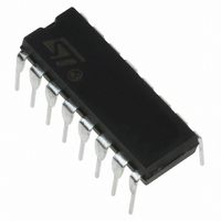
ST7FLIT15BY0B6 STMicroelectronics, ST7FLIT15BY0B6 Datasheet - Page 121

ST7FLIT15BY0B6
Manufacturer Part Number
ST7FLIT15BY0B6
Description
IC MCU 8BIT 2K FLASH 16-DIP
Manufacturer
STMicroelectronics
Series
ST7r
Datasheet
1.ST7FLIT15BY1M6.pdf
(159 pages)
Specifications of ST7FLIT15BY0B6
Core Processor
ST7
Core Size
8-Bit
Speed
8MHz
Connectivity
SPI
Peripherals
LVD, POR, PWM, WDT
Number Of I /o
11
Program Memory Size
2KB (2K x 8)
Program Memory Type
FLASH
Ram Size
256 x 8
Voltage - Supply (vcc/vdd)
2.7 V ~ 5.5 V
Data Converters
A/D 7x10b
Oscillator Type
Internal
Operating Temperature
-40°C ~ 85°C
Package / Case
16-DIP (0.300", 7.62mm)
Processor Series
ST7FLIT1x
Core
ST7
Data Bus Width
8 bit
Data Ram Size
256 B
Interface Type
SPI
Maximum Clock Frequency
8 MHz
Number Of Programmable I/os
17
Number Of Timers
4
Maximum Operating Temperature
+ 85 C
Mounting Style
Through Hole
Development Tools By Supplier
ST7FLITE-SK/RAIS, ST7MDT10-DVP3, ST7MDT10-EMU3, STX-RLINK
Minimum Operating Temperature
- 40 C
On-chip Adc
10 bit, 7 Channel
For Use With
497-8427 - BOARD DEMO USB LI-ION ST7260E2497-5049 - KIT STARTER RAISONANCE ST7FLITE
Lead Free Status / RoHS Status
Lead free / RoHS Compliant
Eeprom Size
-
Lead Free Status / Rohs Status
Details
13.4 SUPPLY CURRENT CHARACTERISTICS
The following current consumption specified for
the ST7 functional operating modes over tempera-
ture range does not take into account the clock
source current consumption. To get the total de-
13.4.1 Supply Current
T
Notes:
1. CPU running with memory access, all I/O pins in input mode with a static value at V
in reset state; clock input (CLKIN) driven by external square wave, LVD disabled.
2. All I/O pins in input mode with a static value at V
driven by external square wave, LVD disabled.
3. SLOW mode selected with f
V
4. SLOW-WAIT mode selected with f
V
5. All I/O pins in output mode with a static value at V
tested in production at V
6. All I/O pins in input mode with a static value at V
max.
7. This consumption refers to the Halt period only and not the associated run period which is software dependent.
Figure 71. Typical I
Symbol
Note: Graph displays data beyond the normal operating range of 3V - 5.5V
SS
DD
A
I
DD
= -40 to +85°C unless otherwise specified
(no load), all peripherals in reset state; clock input (CLKIN) driven by external square wave, LVD disabled.
or V
9
8
7
6
5
4
3
2
1
0
2
SS
Supply current in RUN mode
Supply current in WAIT mode
Supply current in SLOW mode
Supply current in SLOW WAIT mode7
Supply current in HALT mode
Supply current in AWUFH mode
(no load), all peripherals in reset state; clock input (CLKIN) driven by external square wave, LVD disabled.
2.5
.5
1
2
4
6
8
3
3.5
DD
Parameter
DD
in RUN vs. f
4
max and f
Vdd (V)
CPU
4.5
based on f
5
CPU
CPU
5)
5.5
CPU
based on f
max.
6)7)
OSC
6
divided by 32. All I/O pins in input mode with a static value at V
6.5
DD
DD
SS
OSC
or V
or V
(no load), LVD disabled. Data based on characterization results,
divided by 32. All I/O pins in input mode with a static value at
f
f
f
f
-40°C≤T
-40°C≤T
SS
CPU
CPU
CPU
CPU
SS
(no load), all peripherals in reset state; clock input (CLKIN)
(no load). Data tested in production at V
vice consumption, the two current values must be
added (except for HALT mode for which the clock
is stopped).
Figure 72. Typical I
=8MHz
=8MHz
=250kHz
=250kHz
Note: Graph displays data beyond the normal operating range of 3V - 5.5V
Note: Graph displays data beyond the normal operating range of 3V - 5.5V
9
8
7
6
5
4
3
2
1
0
Conditions
2
A
A
≤+125°C
≤+125°C
1)
2)
2.5
3)
4)
3
3.5
DD
DD
or V
4
in RUN at f
Vdd (V)
SS
7
3
0.7
0.5
<1
20
4.5
Typ
(no load), all peripherals
5
DD
ST7LITE1xB
9
3.6
0.9
0.8
6
CPU
Max
max. and f
5.5
= 8MHz
140°C
90°C
25°C
-5°C
-45°C
6
121/159
Unit
mA
μA
DD
CPU
6.5
or


