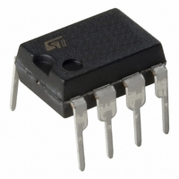
ST7FLITEUS5B6 STMicroelectronics, ST7FLITEUS5B6 Datasheet - Page 60

ST7FLITEUS5B6
Manufacturer Part Number
ST7FLITEUS5B6
Description
MCU 8BIT 1KB FLASH 128KB 8-DIP
Manufacturer
STMicroelectronics
Series
ST7r
Datasheet
1.STEVAL-IFS006V1.pdf
(136 pages)
Specifications of ST7FLITEUS5B6
Core Processor
ST7
Core Size
8-Bit
Speed
8MHz
Peripherals
LVD, POR, PWM, WDT
Number Of I /o
5
Program Memory Size
1KB (1K x 8)
Program Memory Type
FLASH
Ram Size
128 x 8
Voltage - Supply (vcc/vdd)
2.4 V ~ 5.5 V
Data Converters
A/D 5x10b
Oscillator Type
Internal
Operating Temperature
-40°C ~ 85°C
Package / Case
8-DIP (0.300", 7.62mm)
Controller Family/series
ST7
No. Of I/o's
5
Ram Memory Size
128Byte
Cpu Speed
8MHz
No. Of Timers
2
Rohs Compliant
Yes
For Use With
497-6403 - BOARD EVAL 8BIT MICRO + TDE1708497-6407 - BOARD EVAL FOR VACUUM CLEANER497-5861 - EVAL BRD POWER MOSFET/8PIN MCU497-5858 - EVAL BOARD PLAYBACK ST7FLITE497-5515 - EVAL BOARD PHASE CTRL DIMMER497-5049 - KIT STARTER RAISONANCE ST7FLITE497-5046 - KIT TOOL FOR ST7/UPSD/STR7 MCU
Lead Free Status / RoHS Status
Lead free / RoHS Compliant
Eeprom Size
-
Connectivity
-
Other names
497-5636-5
Available stocks
Company
Part Number
Manufacturer
Quantity
Price
Company:
Part Number:
ST7FLITEUS5B6
Manufacturer:
STMicroelectronics
Quantity:
8
I/O ports
Caution:
9.2.2
60/136
Spurious interrupts
When enabling/disabling an external interrupt by setting/resetting the related OR register bit,
a spurious interrupt is generated if the pin level is low and its edge sensitivity includes
falling/rising edge. This is due to the edge detector input which is switched to '1' when the
external interrupt is disabled by the OR register.
To avoid this unwanted interrupt, a "safe" edge sensitivity (rising edge for enabling and
falling edge for disabling) has to be selected before changing the OR register bit and
configuring the appropriate sensitivity again.
In case a pin level change occurs during these operations (asynchronous signal input), as
interrupts are generated according to the current sensitivity, it is advised to disable all
interrupts before and to reenable them after the complete previous sequence in order to
avoid an external interrupt occurring on the unwanted edge.
This corresponds to the following steps:
1.
2. To disable an external interrupt:
Output modes
The output configuration is selected by setting the corresponding DDR register bit. In this
case, writing the DR register applies this digital value to the I/O pin through the latch. Then
reading the DR register returns the previously stored value.
Two different output modes can be selected by software through the OR register: Output
push-pull and open-drain.
Table 17.
1. When switching from input to output mode, the DR register has to be written first to drive the correct level
on the pin as soon as the port is configured as an output.
To enable an external interrupt:
a)
b)
c)
d)
e)
a)
b)
c)
d)
DR
0
1
Set the interrupt mask with the SIM instruction (in cases where a pin level change
could occur)
Select rising edge
Enable the external interrupt through the OR register
Select the desired sensitivity if different from rising edge
Reset the interrupt mask with the RIM instruction (in cases where a pin level
change could occur)
Set the interrupt mask with the SIM instruction SIM (in cases where a pin level
change could occur)
Select falling edge
Disable the external interrupt through the OR register
Select rising edge
DR register value and output pin status
Push-pull
V
V
SS
DD
(1)
ST7LITEUS2, ST7LITEUS5
Open-drain
Floating
V
SS


