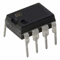
ST7FLITEUS5B6 STMicroelectronics, ST7FLITEUS5B6 Datasheet - Page 79

ST7FLITEUS5B6
Manufacturer Part Number
ST7FLITEUS5B6
Description
MCU 8BIT 1KB FLASH 128KB 8-DIP
Manufacturer
STMicroelectronics
Series
ST7r
Datasheet
1.STEVAL-IFS006V1.pdf
(136 pages)
Specifications of ST7FLITEUS5B6
Core Processor
ST7
Core Size
8-Bit
Speed
8MHz
Peripherals
LVD, POR, PWM, WDT
Number Of I /o
5
Program Memory Size
1KB (1K x 8)
Program Memory Type
FLASH
Ram Size
128 x 8
Voltage - Supply (vcc/vdd)
2.4 V ~ 5.5 V
Data Converters
A/D 5x10b
Oscillator Type
Internal
Operating Temperature
-40°C ~ 85°C
Package / Case
8-DIP (0.300", 7.62mm)
Controller Family/series
ST7
No. Of I/o's
5
Ram Memory Size
128Byte
Cpu Speed
8MHz
No. Of Timers
2
Rohs Compliant
Yes
For Use With
497-6403 - BOARD EVAL 8BIT MICRO + TDE1708497-6407 - BOARD EVAL FOR VACUUM CLEANER497-5861 - EVAL BRD POWER MOSFET/8PIN MCU497-5858 - EVAL BOARD PLAYBACK ST7FLITE497-5515 - EVAL BOARD PHASE CTRL DIMMER497-5049 - KIT STARTER RAISONANCE ST7FLITE497-5046 - KIT TOOL FOR ST7/UPSD/STR7 MCU
Lead Free Status / RoHS Status
Lead free / RoHS Compliant
Eeprom Size
-
Connectivity
-
Other names
497-5636-5
Available stocks
Company
Part Number
Manufacturer
Quantity
Price
Company:
Part Number:
ST7FLITEUS5B6
Manufacturer:
STMicroelectronics
Quantity:
8
ST7LITEUS2, ST7LITEUS5
10.3
10.3.1
10.3.2
10.3.3
10-bit A/D converter (ADC)
Introduction
The on-chip Analog to Digital Converter (ADC) peripheral is a 10-bit, successive
approximation converter with internal sample and hold circuitry. This peripheral has up to 5
multiplexed analog input channels (refer to device pin out description) that allow the
peripheral to convert the analog voltage levels from up to 5 different sources.
The result of the conversion is stored in a 10-bit Data register. The A/D converter is
controlled through a Control/Status register.
Main features
●
●
●
●
●
●
The block diagram is shown in
Functional description
Analog power supply
V
device pin out description) they are internally connected to the V
Conversion accuracy may therefore be impacted by voltage drops and noise in the event of
heavily loaded or badly decoupled power supply lines.
DDA
10-bit conversion
Up to 5 channels with multiplexed input
Linear successive approximation
Data register (DR) which contains the results
Conversion complete status flag
On/off bit (to reduce consumption)
and V
SSA
are the high and low level reference voltage pins. In some devices (refer to
Figure
36.
DD
and V
On-chip peripherals
SS
pins.
79/136


