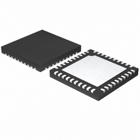
ST72F63BK2U1TR STMicroelectronics, ST72F63BK2U1TR Datasheet - Page 126

ST72F63BK2U1TR
Manufacturer Part Number
ST72F63BK2U1TR
Description
IC MCU 8BIT 8K FLASH 40-QFN
Manufacturer
STMicroelectronics
Series
ST7r
Datasheet
1.ST72F63BD6U1TR.pdf
(186 pages)
Specifications of ST72F63BK2U1TR
Core Processor
ST7
Core Size
8-Bit
Speed
8MHz
Connectivity
I²C, SCI, USB
Peripherals
DMA, LVD, POR, PWM, WDT
Number Of I /o
19
Program Memory Size
8KB (8K x 8)
Program Memory Type
FLASH
Ram Size
384 x 8
Voltage - Supply (vcc/vdd)
4 V ~ 5.5 V
Data Converters
A/D 12x8b
Oscillator Type
External
Operating Temperature
0°C ~ 70°C
Package / Case
40-QFN
Processor Series
ST72F6x
Core
ST7
Data Bus Width
8 bit
Data Ram Size
384 B
Interface Type
I2C, SCI
Maximum Clock Frequency
8 MHz
Number Of Programmable I/os
19
Number Of Timers
2
Maximum Operating Temperature
+ 70 C
Mounting Style
SMD/SMT
Development Tools By Supplier
ST7MDTU3-EPB/US, ST72F63B-SK/RAIS, ST7MDTU3-EMU3, STX-RLINK
Minimum Operating Temperature
0 C
On-chip Adc
8 bit, 8 Channel / 8 bit, 12 Channel
Lead Free Status / RoHS Status
Lead free / RoHS Compliant
Eeprom Size
-
Lead Free Status / Rohs Status
Details
Available stocks
Company
Part Number
Manufacturer
Quantity
Price
- Current page: 126 of 186
- Download datasheet (3Mb)
On-chip peripherals
126/186
Figure 50. ADC block diagram
Digital A/D conversion result
The conversion is monotonic, meaning that the result never decreases if the analog input
does not and never increases if the analog input does not.
If the input voltage (V
the conversion result in the DR register is FFh (full scale) without overflow indication.
If input voltage (V
conversion result in the DR register is 00h.
The A/D converter is linear and the digital result of the conversion is stored in the ADCDR
register. The accuracy of the conversion is described in the parametric section.
R
is too high, this will result in a loss of accuracy due to leakage and sampling not being
completed in the allotted time.
A/D conversion phases
The A/D conversion is based on two conversion phases as shown in
●
●
While the ADC is on, these two phases are continuously repeated.
At the end of each conversion, the sample capacitor is kept loaded with the previous
measurement load. The advantage of this behavior is that it minimizes the current
consumption on the analog pin in case of single input channel measurement.
AIN
Sample capacitor loading [duration: t
During this phase, the V
sample capacitor.
A/D conversion [duration: t
During this phase, the A/D conversion is computed (8 successive approximations
cycles) and the C
the optimum analog to digital conversion accuracy.
is the maximum recommended impedance for an analog input signal. If the impedance
AIN0
AIN1
AINx
AIN
COCO
) is lower than or equal to V
AIN
ADC
ANALOG
) is greater than or equal to V
MUX
0
sample capacitor is disconnected from the analog input pin to get
ADON
AIN
4
Doc ID 7516 Rev 8
R
CONV
f
CPU
input voltage to be measured is loaded into the C
ADC
ADCDR
0
CH3
]
CH2
LOAD
D7
HOLD CONTROL
CH1
DIV 4
D6
]
SSA
CH0
C
ADC
D5
(low-level voltage reference) then the
DDA
ADCCSR
D4
(high-level voltage reference) then
ANALOG TO DIGITAL
D3
f
ADC
CONVERTER
D2
D1
Figure
D0
51:
ST7263Bxx
ADC
Related parts for ST72F63BK2U1TR
Image
Part Number
Description
Manufacturer
Datasheet
Request
R

Part Number:
Description:
KIT STARTER LOW COST ST7
Manufacturer:
STMicroelectronics
Datasheet:

Part Number:
Description:
STMicroelectronics [RIPPLE-CARRY BINARY COUNTER/DIVIDERS]
Manufacturer:
STMicroelectronics
Datasheet:

Part Number:
Description:
STMicroelectronics [LIQUID-CRYSTAL DISPLAY DRIVERS]
Manufacturer:
STMicroelectronics
Datasheet:

Part Number:
Description:
BOARD EVAL FOR MEMS SENSORS
Manufacturer:
STMicroelectronics
Datasheet:

Part Number:
Description:
NPN TRANSISTOR POWER MODULE
Manufacturer:
STMicroelectronics
Datasheet:

Part Number:
Description:
TURBOSWITCH ULTRA-FAST HIGH VOLTAGE DIODE
Manufacturer:
STMicroelectronics
Datasheet:

Part Number:
Description:
Manufacturer:
STMicroelectronics
Datasheet:

Part Number:
Description:
DIODE / SCR MODULE
Manufacturer:
STMicroelectronics
Datasheet:

Part Number:
Description:
DIODE / SCR MODULE
Manufacturer:
STMicroelectronics
Datasheet:

Part Number:
Description:
Search -----> STE16N100
Manufacturer:
STMicroelectronics
Datasheet:

Part Number:
Description:
Search ---> STE53NA50
Manufacturer:
STMicroelectronics
Datasheet:

Part Number:
Description:
NPN Transistor Power Module
Manufacturer:
STMicroelectronics
Datasheet:


