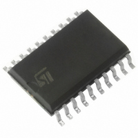
ST7FLITE35F2M6 STMicroelectronics, ST7FLITE35F2M6 Datasheet - Page 162

ST7FLITE35F2M6
Manufacturer Part Number
ST7FLITE35F2M6
Description
IC MCU 8BIT 8K FLASH 20SOIC
Manufacturer
STMicroelectronics
Series
ST7r
Specifications of ST7FLITE35F2M6
Core Processor
ST7
Core Size
8-Bit
Speed
8MHz
Connectivity
LINSCI, SPI
Peripherals
LVD, POR, PWM, WDT
Number Of I /o
15
Program Memory Size
8KB (8K x 8)
Program Memory Type
FLASH
Ram Size
384 x 8
Voltage - Supply (vcc/vdd)
2.7 V ~ 5.5 V
Data Converters
A/D 7x10b
Oscillator Type
Internal
Operating Temperature
-40°C ~ 85°C
Package / Case
20-SOIC (7.5mm Width)
Processor Series
ST7FLITE3x
Core
ST7
Data Bus Width
8 bit
Data Ram Size
384 B
Interface Type
LINSCI, SPI
Maximum Clock Frequency
8 MHz
Number Of Programmable I/os
15
Number Of Timers
4
Operating Supply Voltage
2.7 V to 5.5 V
Maximum Operating Temperature
+ 125 C
Mounting Style
SMD/SMT
Development Tools By Supplier
ST7FLITE-SK/RAIS, ST7MDT10-DVP3, ST7MDT10-EMU3, STX-RLINK
Minimum Operating Temperature
- 40 C
On-chip Adc
10 bit, 7 Channel
For Use With
497-5858 - EVAL BOARD PLAYBACK ST7FLITE497-5085 - EVAL BOARD UNIV MOTOR CONTROL497-5049 - KIT STARTER RAISONANCE ST7FLITE
Lead Free Status / RoHS Status
Lead free / RoHS Compliant
Eeprom Size
-
Lead Free Status / Rohs Status
Details
Available stocks
Company
Part Number
Manufacturer
Quantity
Price
Part Number:
ST7FLITE35F2M6TR
Manufacturer:
ST
Quantity:
20 000
ST7LITE3xF2
OPTION BYTES (Cont’d)
OPTION BYTE 1
OPT 7 = PLLx4x8 PLL Factor Selection.
0: PLLx4
1: PLLx8
OPT 6 = PLLOFF PLL Disable
This option bit enables or disables the PLL.
0: PLL enabled
1: PLL disabled (bypassed)
OPT 5 = Reserved. Must always be set to 1.
OPT 4 = OSC RC Oscillator Selection
This option bit enables to select the internal RC
Oscillator.
0: RC Oscillator on
1: RC Oscillator off
Notes:
– RC oscillator available on ST7LITE35 and
– If the RC oscillator is selected, then to improve
162/173
Default
Value
ST7LITE39 devices only
clock stability and frequency accuracy, it is rec-
ommended to place a decoupling capacitor, typ-
ically 100nF, between the V
close as possible to the ST7 device.
AWU
CK
1
7
1
OSCRANGE
2:0
1
OPTION BYTE 0
1
DD
SEC1 SEC0 FMPR FMPW
and V
1
SS
1
pins as
0
0
0
OPT 3:2 = LVD[1:0] Low Voltage Selection
These option bits enable the voltage detection
block (LVD and AVD) with a selected threshold to
the LVD and AVD.
OPT 1 = WDGSW Hardware or Software Watch-
dog
0: Hardware (watchdog always enabled)
1: Software (watchdog to be enabled by software)
OPT 0 = WDG HALT Watchdog Reset on Halt
0: No reset generation when entering HALT mode
1: Reset generation when entering HALT mode
LVD Off
Highest Voltage Threshold
Medium Voltage Threshold
Lowest Voltage Threshold
x4x8
PLL
1
7
OFF
PLL
1
Configuration
Res. OSC
1
OPTION BYTE 1
0
1
LVD
1:0
1
WDG
VD1
SW
1
1
0
0
1
HALT
WDG
VD0
0
1
0
1
0
1


