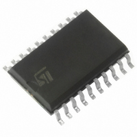
ST7FLITE35F2M6 STMicroelectronics, ST7FLITE35F2M6 Datasheet - Page 95

ST7FLITE35F2M6
Manufacturer Part Number
ST7FLITE35F2M6
Description
IC MCU 8BIT 8K FLASH 20SOIC
Manufacturer
STMicroelectronics
Series
ST7r
Specifications of ST7FLITE35F2M6
Core Processor
ST7
Core Size
8-Bit
Speed
8MHz
Connectivity
LINSCI, SPI
Peripherals
LVD, POR, PWM, WDT
Number Of I /o
15
Program Memory Size
8KB (8K x 8)
Program Memory Type
FLASH
Ram Size
384 x 8
Voltage - Supply (vcc/vdd)
2.7 V ~ 5.5 V
Data Converters
A/D 7x10b
Oscillator Type
Internal
Operating Temperature
-40°C ~ 85°C
Package / Case
20-SOIC (7.5mm Width)
Processor Series
ST7FLITE3x
Core
ST7
Data Bus Width
8 bit
Data Ram Size
384 B
Interface Type
LINSCI, SPI
Maximum Clock Frequency
8 MHz
Number Of Programmable I/os
15
Number Of Timers
4
Operating Supply Voltage
2.7 V to 5.5 V
Maximum Operating Temperature
+ 125 C
Mounting Style
SMD/SMT
Development Tools By Supplier
ST7FLITE-SK/RAIS, ST7MDT10-DVP3, ST7MDT10-EMU3, STX-RLINK
Minimum Operating Temperature
- 40 C
On-chip Adc
10 bit, 7 Channel
For Use With
497-5858 - EVAL BOARD PLAYBACK ST7FLITE497-5085 - EVAL BOARD UNIV MOTOR CONTROL497-5049 - KIT STARTER RAISONANCE ST7FLITE
Lead Free Status / RoHS Status
Lead free / RoHS Compliant
Eeprom Size
-
Lead Free Status / Rohs Status
Details
Available stocks
Company
Part Number
Manufacturer
Quantity
Price
Part Number:
ST7FLITE35F2M6TR
Manufacturer:
ST
Quantity:
20 000
LINSCI™ SERIAL COMMUNICATION INTERFACE (SCI Mode) (cont’d)
11.5.5.3 Receiver
The SCI can receive data words of either 8 or 9
bits. When the M bit is set, word length is 9 bits
and the MSB is stored in the R8 bit in the SCICR1
register.
Character reception
During a SCI reception, data shifts in least signifi-
cant bit first through the RDI pin. In this mode, the
SCIDR register consists or a buffer (RDR) be-
tween the internal bus and the received shift regis-
ter (see
Procedure
– Select the M bit to define the word length.
– Select the desired baud rate using the SCIBRR
– Set the RE bit, this enables the receiver which
When a character is received:
– The RDRF bit is set. It indicates that the content
– An interrupt is generated if the RIE bit is set and
– The error flags can be set if a frame error, noise
Clearing the RDRF bit is performed by the following
software sequence done by:
1. An access to the SCISR register
2. A read to the SCIDR register.
The RDRF bit must be cleared before the end of the
reception of the next character to avoid an overrun
error.
Idle Line
When an idle line is detected, there is the same
procedure as a data received character plus an in-
terrupt if the ILIE bit is set and the I[|1:0] bits are
cleared in the CCR register.
Overrun Error
An overrun error occurs when a character is re-
ceived when RDRF has not been reset. Data can
not be transferred from the shift register to the
TDR register as long as the RDRF bit is not
cleared.
When an overrun error occurs:
and the SCIERPR registers.
begins searching for a start bit.
of the shift register is transferred to the RDR.
the I[1:0] bits are cleared in the CCR register.
or an overrun error has been detected during re-
ception.
Figure
55).
– The OR bit is set.
– The RDR content will not be lost.
– The shift register will be overwritten.
– An interrupt is generated if the RIE bit is set and
The OR bit is reset by an access to the SCISR reg-
ister followed by a SCIDR register read operation.
Noise Error
Oversampling techniques are used for data recov-
ery by discriminating between valid incoming data
and noise.
When noise is detected in a character:
– The NF bit is set at the rising edge of the RDRF
– Data is transferred from the Shift register to the
– No interrupt is generated. However this bit rises
The NF bit is reset by a SCISR register read oper-
ation followed by a SCIDR register read operation.
Framing Error
A framing error is detected when:
– The stop bit is not recognized on reception at the
– A break is received.
When the framing error is detected:
– the FE bit is set by hardware
– Data is transferred from the Shift register to the
– No interrupt is generated. However this bit rises
The FE bit is reset by a SCISR register read oper-
ation followed by a SCIDR register read operation.
Break Character
– When a break character is received, the SCI
the I[|1:0] bits are cleared in the CCR register.
bit.
SCIDR register.
at the same time as the RDRF bit which itself
generates an interrupt.
expected time, following either a desynchroniza-
tion or excessive noise.
SCIDR register.
at the same time as the RDRF bit which itself
generates an interrupt.
handles it as a framing error. To differentiate a
break character from a framing error, it is neces-
sary to read the SCIDR. If the received value is
00h, it is a break character. Otherwise it is a
framing error.
ST7LITE3xF2
95/173
1


