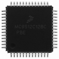
MC9S12C128CPBE Freescale Semiconductor, MC9S12C128CPBE Datasheet - Page 357

MC9S12C128CPBE
Manufacturer Part Number
MC9S12C128CPBE
Description
IC MCU 128K FLASH 25MHZ 52-LQFP
Manufacturer
Freescale Semiconductor
Series
HCS12r
Specifications of MC9S12C128CPBE
Core Processor
HCS12
Core Size
16-Bit
Speed
25MHz
Connectivity
CAN, EBI/EMI, SCI, SPI
Peripherals
POR, PWM, WDT
Number Of I /o
35
Program Memory Size
128KB (128K x 8)
Program Memory Type
FLASH
Ram Size
4K x 8
Voltage - Supply (vcc/vdd)
2.35 V ~ 5.5 V
Data Converters
A/D 8x10b
Oscillator Type
Internal
Operating Temperature
-40°C ~ 85°C
Package / Case
52-LQFP
Lead Free Status / RoHS Status
Lead free / RoHS Compliant
Eeprom Size
-
Available stocks
Company
Part Number
Manufacturer
Quantity
Price
Company:
Part Number:
MC9S12C128CPBE
Manufacturer:
Freescale Semiconductor
Quantity:
10 000
Company:
Part Number:
MC9S12C128CPBER
Manufacturer:
Freescale Semiconductor
Quantity:
10 000
- Current page: 357 of 690
- Download datasheet (4Mb)
12.3.2.5
The PWMCAE register contains six control bits for the selection of center aligned outputs or left aligned
outputs for each PWM channel. If the CAEx bit is set to a 1, the corresponding PWM output will be center
aligned. If the CAEx bit is cleared, the corresponding PWM output will be left aligned. Reference
Section 12.4.2.5, “Left Aligned Outputs,”
detailed description of the PWM output modes.
Freescale Semiconductor
PCKB[2:0]
PCKA[2:0]
Field
6:5
2:0
Prescaler Select for Clock B — Clock B is 1 of two clock sources which can be used for channels 2 or 3. These
three bits determine the rate of clock B, as shown in
Prescaler Select for Clock A — Clock A is 1 of two clock sources which can be used for channels 0, 1, 4, or 5.
These three bits determine the rate of clock A, as shown in
PWM Center Align Enable Register (PWMCAE)
PCKB2
PCKA2
0
0
0
0
1
1
1
1
0
0
0
0
1
1
1
1
Table 12-5. PWMPRCLK Field Descriptions
Table 12-6. Clock B Prescaler Selects
Table 12-7. Clock A Prescaler Selects
MC9S12C-Family / MC9S12GC-Family
PCKB1
PCKA1
0
0
1
1
0
0
1
1
0
0
1
1
0
0
1
1
and
Section 12.4.2.6, “Center Aligned Outputs,”
Rev 01.24
PCKB0
PCKA0
Chapter 12 Pulse-Width Modulator (PWM8B6CV1) Block Description
0
1
0
1
0
1
0
1
0
1
0
1
0
1
0
1
Description
Table
12-6.
Table
Value of Clock B
Value of Clock A
Bus Clock / 128
Bus Clock / 128
12-7.
Bus Clock / 16
Bus Clock / 32
Bus Clock / 16
Bus Clock / 32
Bus Clock / 64
Bus Clock / 64
Bus Clock / 2
Bus Clock / 4
Bus Clock / 8
Bus Clock / 2
Bus Clock / 4
Bus Clock / 8
Bus Clock
Bus Clock
for a more
357
Related parts for MC9S12C128CPBE
Image
Part Number
Description
Manufacturer
Datasheet
Request
R
Part Number:
Description:
Manufacturer:
Freescale Semiconductor, Inc
Datasheet:
Part Number:
Description:
Manufacturer:
Freescale Semiconductor, Inc
Datasheet:
Part Number:
Description:
Manufacturer:
Freescale Semiconductor, Inc
Datasheet:
Part Number:
Description:
Manufacturer:
Freescale Semiconductor, Inc
Datasheet:
Part Number:
Description:
Manufacturer:
Freescale Semiconductor, Inc
Datasheet:
Part Number:
Description:
Manufacturer:
Freescale Semiconductor, Inc
Datasheet:
Part Number:
Description:
Manufacturer:
Freescale Semiconductor, Inc
Datasheet:
Part Number:
Description:
Manufacturer:
Freescale Semiconductor, Inc
Datasheet:
Part Number:
Description:
Manufacturer:
Freescale Semiconductor, Inc
Datasheet:
Part Number:
Description:
Manufacturer:
Freescale Semiconductor, Inc
Datasheet:
Part Number:
Description:
Manufacturer:
Freescale Semiconductor, Inc
Datasheet:
Part Number:
Description:
Manufacturer:
Freescale Semiconductor, Inc
Datasheet:
Part Number:
Description:
Manufacturer:
Freescale Semiconductor, Inc
Datasheet:
Part Number:
Description:
Manufacturer:
Freescale Semiconductor, Inc
Datasheet:
Part Number:
Description:
Manufacturer:
Freescale Semiconductor, Inc
Datasheet:


