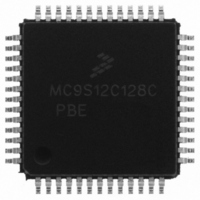
MC9S12C128CPBE Freescale Semiconductor, MC9S12C128CPBE Datasheet - Page 468

MC9S12C128CPBE
Manufacturer Part Number
MC9S12C128CPBE
Description
IC MCU 128K FLASH 25MHZ 52-LQFP
Manufacturer
Freescale Semiconductor
Series
HCS12r
Specifications of MC9S12C128CPBE
Core Processor
HCS12
Core Size
16-Bit
Speed
25MHz
Connectivity
CAN, EBI/EMI, SCI, SPI
Peripherals
POR, PWM, WDT
Number Of I /o
35
Program Memory Size
128KB (128K x 8)
Program Memory Type
FLASH
Ram Size
4K x 8
Voltage - Supply (vcc/vdd)
2.35 V ~ 5.5 V
Data Converters
A/D 8x10b
Oscillator Type
Internal
Operating Temperature
-40°C ~ 85°C
Package / Case
52-LQFP
Lead Free Status / RoHS Status
Lead free / RoHS Compliant
Eeprom Size
-
Available stocks
Company
Part Number
Manufacturer
Quantity
Price
Company:
Part Number:
MC9S12C128CPBE
Manufacturer:
Freescale Semiconductor
Quantity:
10 000
Company:
Part Number:
MC9S12C128CPBER
Manufacturer:
Freescale Semiconductor
Quantity:
10 000
- Current page: 468 of 690
- Download datasheet (4Mb)
Chapter 16 Dual Output Voltage Regulator (VREG3V3V2) Block Description
16.4.1
VREG3V3V2, respectively its regulator core has two parallel, independent regulation loops (REG1 and
REG2) that differ only in the amount of current that can be sourced to the connected loads. Therefore, only
REG1 providing the supply at V
The regulator is a linear series regulator with a bandgap reference in its Full Performance Mode and a
voltage clamp in Reduced Power Mode. All load currents flow from input V
reference circuits are connected to V
16.4.2
In Full Performance Mode, a fraction of the output voltage (V
fed to an operational amplifier. The amplified input voltage difference controls the gate of an output driver
which basically is a large NMOS transistor connected to the output.
16.4.3
In Reduced Power Mode, the driver gate is connected to a buffered fraction of the input voltage (V
The operational amplifier and the bandgap are disabled to reduce power consumption.
16.4.4
sub-block LVD is responsible for generating the low-voltage interrupt (LVI). LVD monitors the input
voltage (V
status flag LVDS changes its value. The LVD is available in FPM and is inactive in Reduced Power Mode
and Shutdown Mode.
16.4.5
This functional block monitors output V
V
Due to its role during chip power-up this module must be active in all operating modes of VREG3V3V2.
16.4.6
Block LVR monitors the primary output voltage V
LVR asserts and when rising above the deassertion level (V
function is available only in Full Performance Mode.
16.4.7
This part contains the register block of VREG3V3V2 and further digital functionality needed to control
the operating modes. CTRL also represents the interface to the digital core logic.
468
PORD
, the signal goes low. The transition to low forces the CPU in the power-on sequence.
DDA
REG — Regulator Core
Full-Performance Mode
Reduced-Power Mode
LVD — Low-Voltage Detect
POR — Power-On Reset
LVR — Low-Voltage Reset
CTRL — Regulator Control
–V
SSA
) and continuously updates the status flag LVDS. Interrupt flag LVIF is set whenever
DD
/V
MC9S12C-Family / MC9S12GC-Family
DDA
SS
DD
is explained. The principle is also valid for REG2.
and V
. If V
SSA
Rev 01.24
DD
DD
.
is below V
. If it drops below the assertion level (V
LVRD
DD
PORD
) and the bandgap reference voltage are
) signal LVR negates again. The LVR
, signal POR is high, if it exceeds
DDR
to V
Freescale Semiconductor
SS
or V
LVRA
SSPLL
) signal
DDR
, the
).
Related parts for MC9S12C128CPBE
Image
Part Number
Description
Manufacturer
Datasheet
Request
R
Part Number:
Description:
Manufacturer:
Freescale Semiconductor, Inc
Datasheet:
Part Number:
Description:
Manufacturer:
Freescale Semiconductor, Inc
Datasheet:
Part Number:
Description:
Manufacturer:
Freescale Semiconductor, Inc
Datasheet:
Part Number:
Description:
Manufacturer:
Freescale Semiconductor, Inc
Datasheet:
Part Number:
Description:
Manufacturer:
Freescale Semiconductor, Inc
Datasheet:
Part Number:
Description:
Manufacturer:
Freescale Semiconductor, Inc
Datasheet:
Part Number:
Description:
Manufacturer:
Freescale Semiconductor, Inc
Datasheet:
Part Number:
Description:
Manufacturer:
Freescale Semiconductor, Inc
Datasheet:
Part Number:
Description:
Manufacturer:
Freescale Semiconductor, Inc
Datasheet:
Part Number:
Description:
Manufacturer:
Freescale Semiconductor, Inc
Datasheet:
Part Number:
Description:
Manufacturer:
Freescale Semiconductor, Inc
Datasheet:
Part Number:
Description:
Manufacturer:
Freescale Semiconductor, Inc
Datasheet:
Part Number:
Description:
Manufacturer:
Freescale Semiconductor, Inc
Datasheet:
Part Number:
Description:
Manufacturer:
Freescale Semiconductor, Inc
Datasheet:
Part Number:
Description:
Manufacturer:
Freescale Semiconductor, Inc
Datasheet:


