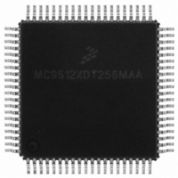
MC9S12XDT256MAA Freescale Semiconductor, MC9S12XDT256MAA Datasheet - Page 211

MC9S12XDT256MAA
Manufacturer Part Number
MC9S12XDT256MAA
Description
IC MCU 256K FLASH 80-QFP
Manufacturer
Freescale Semiconductor
Series
HCS12r
Datasheet
1.MC9S12XD64CAA.pdf
(1348 pages)
Specifications of MC9S12XDT256MAA
Core Processor
HCS12X
Core Size
16-Bit
Speed
80MHz
Connectivity
CAN, EBI/EMI, I²C, IrDA, LIN, SCI, SPI
Peripherals
LVD, POR, PWM, WDT
Number Of I /o
59
Program Memory Size
256KB (256K x 8)
Program Memory Type
FLASH
Eeprom Size
4K x 8
Ram Size
16K x 8
Voltage - Supply (vcc/vdd)
2.35 V ~ 5.5 V
Data Converters
A/D 8x10b
Oscillator Type
External
Operating Temperature
-40°C ~ 125°C
Package / Case
80-QFP
Cpu Family
HCS12
Device Core Size
16b
Frequency (max)
40MHz
Interface Type
CAN/I2C/SCI/SPI
Total Internal Ram Size
16KB
# I/os (max)
59
Number Of Timers - General Purpose
12
Operating Supply Voltage (typ)
2.5/5V
Operating Supply Voltage (max)
2.75/5.5V
Operating Supply Voltage (min)
2.35/3.15V
On-chip Adc
8-chx10-bit
Instruction Set Architecture
CISC
Operating Temp Range
-40C to 125C
Operating Temperature Classification
Automotive
Mounting
Surface Mount
Pin Count
80
Package Type
PQFP
Processor Series
S12XD
Core
HCS12
Data Bus Width
16 bit
Data Ram Size
16 KB
Maximum Clock Frequency
40 MHz
Number Of Programmable I/os
59
Number Of Timers
12
Operating Supply Voltage
0 V to 5.5 V
Maximum Operating Temperature
+ 125 C
Mounting Style
SMD/SMT
3rd Party Development Tools
EWHCS12
Development Tools By Supplier
EVB9S12XDP512E
Minimum Operating Temperature
- 40 C
Lead Free Status / RoHS Status
Lead free / RoHS Compliant
Available stocks
Company
Part Number
Manufacturer
Quantity
Price
Company:
Part Number:
MC9S12XDT256MAA
Manufacturer:
Freescale Semiconductor
Quantity:
10 000
- Current page: 211 of 1348
- Download datasheet (8Mb)
6.8.1.8
In this mode the result of an operation between two registers is stored in one of the registers used as
operands.
RD = RD RS is the general register to register format, with register RD being the first operand and RS
the second. RD and RS can be any of the 8 general purpose registers R0 … R7. If R0 is used as the
destination register, only the condition code flags are updated. This addressing mode is used only for shift
operations with a variable shift value
Examples:
6.8.1.9
In this mode the result of an operation between two or three registers is stored into a third one.
RD = RS1 RS2 is the general format used in the order RD, RS1, RS1. RD, RS1, RS2 can be any of the
8 general purpose registers R0 … R7. If R0 is used as the destination register RD, only the condition code
flags are updated. This addressing mode is used for all arithmetic and logical operations.
Examples:
6.8.1.10
A 9-bit signed word address offset is included in the instruction word. This addressing mode is used for
conditional branch instructions.
Examples:
6.8.1.11
An 11-bit signed word address offset is included in the instruction word. This addressing mode is used for
the unconditional branch instruction.
Examples:
6.8.1.12
(RS, #offset5) provides an unsigned offset from the base register.
Examples:
Freescale Semiconductor
LSL
LSR
ADC
SUB
BCC
BEQ
BRA
LDB
STW
Dyadic Addressing (DYA)
Triadic Addressing (TRI)
Relative Addressing 9-Bit Wide (REL9)
Relative Addressing 10-Bit Wide (REL10)
Index Register plus Immediate Offset (IDO5)
R4,R5
R4,R5
R5,R6,R7
R5,R6,R7
REL9
REL9
REL10
R4,(R1,#offset)
R4,(R1,#offset)
; R4 = R4 << R5
; R4 = R4 >> R5
MC9S12XDP512 Data Sheet, Rev. 2.21
; R5 = R6 + R7 + Carry
; R5 = R6 - R7
; PC = PC + 2 + (REL9 << 1)
; PC = PC + 2 + (REL9 << 1)
; PC = PC + 2 + (REL10 << 1)
; loads a byte from R1+offset into R4
; stores R4 as a word to R1+offset
Chapter 6 XGATE (S12XGATEV2)
211
Related parts for MC9S12XDT256MAA
Image
Part Number
Description
Manufacturer
Datasheet
Request
R

Part Number:
Description:
16-BIT MICROPROCESSOR FAMILY
Manufacturer:
FREESCALE [Freescale Semiconductor, Inc]
Datasheet:
Part Number:
Description:
Manufacturer:
Freescale Semiconductor, Inc
Datasheet:
Part Number:
Description:
Manufacturer:
Freescale Semiconductor, Inc
Datasheet:
Part Number:
Description:
Manufacturer:
Freescale Semiconductor, Inc
Datasheet:
Part Number:
Description:
Manufacturer:
Freescale Semiconductor, Inc
Datasheet:
Part Number:
Description:
Manufacturer:
Freescale Semiconductor, Inc
Datasheet:
Part Number:
Description:
Manufacturer:
Freescale Semiconductor, Inc
Datasheet:
Part Number:
Description:
Manufacturer:
Freescale Semiconductor, Inc
Datasheet:
Part Number:
Description:
Manufacturer:
Freescale Semiconductor, Inc
Datasheet:
Part Number:
Description:
Manufacturer:
Freescale Semiconductor, Inc
Datasheet:
Part Number:
Description:
Manufacturer:
Freescale Semiconductor, Inc
Datasheet:
Part Number:
Description:
Manufacturer:
Freescale Semiconductor, Inc
Datasheet:
Part Number:
Description:
Manufacturer:
Freescale Semiconductor, Inc
Datasheet:
Part Number:
Description:
Manufacturer:
Freescale Semiconductor, Inc
Datasheet:
Part Number:
Description:
Manufacturer:
Freescale Semiconductor, Inc
Datasheet:


