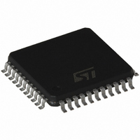
ST7FMC2S6TC STMicroelectronics, ST7FMC2S6TC Datasheet - Page 283

ST7FMC2S6TC
Manufacturer Part Number
ST7FMC2S6TC
Description
IC MCU 8BIT 32K FLASH 44-LQFP
Manufacturer
STMicroelectronics
Series
ST7r
Datasheet
1.ST7FMC2S4T6.pdf
(309 pages)
Specifications of ST7FMC2S6TC
Core Processor
ST7
Core Size
8-Bit
Speed
8MHz
Connectivity
LINSCI, SPI
Peripherals
LVD, Motor Control PWM, POR, PWM, WDT
Number Of I /o
26
Program Memory Size
32KB (32K x 8)
Program Memory Type
FLASH
Ram Size
1K x 8
Voltage - Supply (vcc/vdd)
3.8 V ~ 5.5 V
Data Converters
A/D 16x10b
Oscillator Type
External
Operating Temperature
-40°C ~ 125°C
Package / Case
44-LQFP
For Use With
497-8402 - BOARD EVAL COMPLETE INVERTER497-8400 - KIT IGBT PWR MODULE CTRL ST7MC497-6408 - BOARD EVAL BLDC SENSORLESS MOTOR497-4734 - EVAL KIT 3KW POWER DRIVER BOARD497-4733 - EVAL KIT 1KW POWER DRIVER BOARD497-4732 - EVAL KIT 300W POWER DRIVER BOARD497-4731 - EVAL KIT PWR DRIVER CONTROL BRD
Lead Free Status / RoHS Status
Lead free / RoHS Compliant
Eeprom Size
-
Available stocks
Company
Part Number
Manufacturer
Quantity
Price
Company:
Part Number:
ST7FMC2S6TC
Manufacturer:
STMicroelectronics
Quantity:
10 000
Company:
Part Number:
ST7FMC2S6TCE
Manufacturer:
STMicroelectronics
Quantity:
10 000
- Current page: 283 of 309
- Download datasheet (6Mb)
10-BIT ADC CHARACTERISTICS (Cont’d)
12.14.1 Analog Power Supply and Reference
Pins
Depending on the MCU pin count, the package
may feature separate V
power supply pins. These pins supply power to the
A/D converter cell and function as the high and low
reference voltages for the conversion. In some
packages, V
(refer to
alog supply and reference pads are internally
bonded to the V
Separation of the digital and analog power pins al-
low board designers to improve A/D performance.
Conversion accuracy can be impacted by voltage
drops and noise in the event of heavily loaded or
badly decoupled power supply lines (see
12.14.2 General PCB Design
12.14.2 General PCB Design Guidelines
To obtain best results, some general design and
layout rules should be followed when designing
the application PCB to shield the noise-sensitive,
analog physical interface from noise-generating
CMOS logic signals.
– Use separate digital and analog planes. The an-
Figure 160. Power Supply Filtering
alog ground plane should be connected to the
section 2 on page
AREF
DD
and V
and V
POWER
SUPPLY
SOURCE
V
DD
SSA
SS
AREF
6). In this case the an-
1 to 10μF
pins.
pins are not available
Guidelines).
and V
ST7
DIGITAL NOISE
FILTERING
SSA
EXTERNAL
NOISE
FILTERING
Section
analog
(if needed)
(if needed)
10pF
10pF
0.1μF
0.1μF
– Filter power to the analog power planes. It is rec-
– The analog and digital power supplies should be
– Properly place components and route the signal
digital ground plane via a single point on the
PCB.
ommended to connect capacitors, with good high
frequency characteristics, between the power
and ground lines, placing 0.1µF and optionally, if
needed 10pF capacitors as close as possible to
the ST7 power supply pins and a 1 to 10µF ca-
pacitor close to the power source (see
160).
connected in a star network. Do not use a resis-
tor, as V
the A/D converter and any resistance would
cause a voltage drop and a loss of accuracy.
traces on the PCB to shield the analog inputs.
Analog signals paths should run over the analog
ground plane and be as short as possible. Isolate
analog signals from digital signals that may
switch while the analog inputs are being sampled
by the A/D converter. Do not toggle digital out-
puts on the same I/O port as the A/D input being
converted.
V
V
V
V
SS
DD
AREF
SSA
AREF
ST7MC
is used as a reference voltage by
ST7MC1xx/ST7MC2xx
Figure
283/309
Related parts for ST7FMC2S6TC
Image
Part Number
Description
Manufacturer
Datasheet
Request
R

Part Number:
Description:
STMicroelectronics [RIPPLE-CARRY BINARY COUNTER/DIVIDERS]
Manufacturer:
STMicroelectronics
Datasheet:

Part Number:
Description:
STMicroelectronics [LIQUID-CRYSTAL DISPLAY DRIVERS]
Manufacturer:
STMicroelectronics
Datasheet:

Part Number:
Description:
BOARD EVAL FOR MEMS SENSORS
Manufacturer:
STMicroelectronics
Datasheet:

Part Number:
Description:
NPN TRANSISTOR POWER MODULE
Manufacturer:
STMicroelectronics
Datasheet:

Part Number:
Description:
TURBOSWITCH ULTRA-FAST HIGH VOLTAGE DIODE
Manufacturer:
STMicroelectronics
Datasheet:

Part Number:
Description:
Manufacturer:
STMicroelectronics
Datasheet:

Part Number:
Description:
DIODE / SCR MODULE
Manufacturer:
STMicroelectronics
Datasheet:

Part Number:
Description:
DIODE / SCR MODULE
Manufacturer:
STMicroelectronics
Datasheet:

Part Number:
Description:
Search -----> STE16N100
Manufacturer:
STMicroelectronics
Datasheet:

Part Number:
Description:
Search ---> STE53NA50
Manufacturer:
STMicroelectronics
Datasheet:

Part Number:
Description:
NPN Transistor Power Module
Manufacturer:
STMicroelectronics
Datasheet:

Part Number:
Description:
DIODE / SCR MODULE
Manufacturer:
STMicroelectronics
Datasheet:


