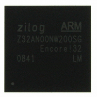
Z32AN00NW200SG Zilog, Z32AN00NW200SG Datasheet - Page 31

Z32AN00NW200SG
Manufacturer Part Number
Z32AN00NW200SG
Description
IC ARM922T MCU 200MHZ 256-BGA
Manufacturer
Zilog
Series
Encore!® 32r
Datasheet
1.Z32AN00NW200SG.pdf
(196 pages)
Specifications of Z32AN00NW200SG
Core Processor
ARM9
Core Size
16/32-Bit
Speed
200MHz
Connectivity
EBI/EMI, IrDA, SmartCard, SPI, UART/USART, USB OTG
Peripherals
DMA, LCD, Magnetic Card Reader, POR, PWM, WDT
Number Of I /o
76
Program Memory Type
ROMless
Ram Size
64K x 8
Voltage - Supply (vcc/vdd)
1.71 V ~ 3.6 V
Data Converters
A/D 4x10b
Oscillator Type
Internal
Operating Temperature
-40°C ~ 85°C
Package / Case
256-LBGA
For Use With
269-4713 - KIT DEV ENCORE 32 SERIES
Lead Free Status / RoHS Status
Lead free / RoHS Compliant
Eeprom Size
-
Program Memory Size
-
Other names
269-4717
Available stocks
Company
Part Number
Manufacturer
Quantity
Price
- Current page: 31 of 196
- Download datasheet (4Mb)
Z32AN Series Data Sheet
5.2
5.3
5.4
5.5
5.5.1
5.5.2
5.5.3
DS0200-003
Accesses
All AHB devices can be accessed with byte, halfword or word accesses. APB devices can be read as bytes
or halfwords, but should only be written with word accesses. Byte or halfword writes to APB devices are
executed as word writes with the defined data being repeated in the other byte lanes to form 32 bits of data.
Example: a byte write of AFh results in a word write of AFAFAFAFh). Byte and halfword reads will operate
properly on all APB devices, but some data may be lost (when reading a 32-bit wide FIFO register, for
example).
Restricted / Reserved Addresses
Accesses to restricted areas will result in a bus error to the requesting device (CPU or DMAC). Addresses
shown as reserved will have no effect and will not result in a bus error.
ROM/SRAM Remapping
Remapping is controlled by a bit in the PMU registers. ROM/SRAM remapping is shown below:
Internal SRAM
The internal SRAM is 64 KB of 0 wait-state memory.
The clock to the SRAM can be disabled via PMU registers to reduce the power consumption of this module
(see System Clocks and Power Management. This clock disable does not disrupt the contents of the
memory.
The internal SRAM can be automatically cleared by writing 1 to bit 0 in INT_SRAM_CLR.CLR. Clearing
takes 64k hclks. During this time, reads of the SRAM are stalled.
Clock Disable
Zeroization
Address FFFF8068h: INT_SRAM_CLR – Internal SRAM Clear Register
31:01
Bits
00
REMAP=0
Type
RW
RO
00000000h - 00007FFFh
00008000h - 0000FFFFh
00400000h - 00407FFFh
00800000h - 0080FFFFh
Reset
REMAP=1
0
0
Address
Description
Reserved
Clear (CLR): When written to ‘1’, hardware writes 0’s to internal SRAM from top
address to zero. When read as ‘0’, the internal clear-to-zero is done. While still set to
‘1’, the clear-to-zero is still in progress. A write of ‘0’ has no effect.
Internal SRAM (64KB)
Internal ROM (32KB)
Internal ROM (32KB)
REMAP = 0
Restricted
Internal SRAM (64KB)
Internal ROM (32KB)
REMAP = 1
Restricted
Page 18
Related parts for Z32AN00NW200SG
Image
Part Number
Description
Manufacturer
Datasheet
Request
R

Part Number:
Description:
Communication Controllers, ZILOG INTELLIGENT PERIPHERAL CONTROLLER (ZIP)
Manufacturer:
Zilog, Inc.
Datasheet:

Part Number:
Description:
KIT DEV FOR Z8 ENCORE 16K TO 64K
Manufacturer:
Zilog
Datasheet:

Part Number:
Description:
KIT DEV Z8 ENCORE XP 28-PIN
Manufacturer:
Zilog
Datasheet:

Part Number:
Description:
DEV KIT FOR Z8 ENCORE 8K/4K
Manufacturer:
Zilog
Datasheet:

Part Number:
Description:
KIT DEV Z8 ENCORE XP 28-PIN
Manufacturer:
Zilog
Datasheet:

Part Number:
Description:
DEV KIT FOR Z8 ENCORE 4K TO 8K
Manufacturer:
Zilog
Datasheet:

Part Number:
Description:
CMOS Z8 microcontroller. ROM 16 Kbytes, RAM 256 bytes, speed 16 MHz, 32 lines I/O, 3.0V to 5.5V
Manufacturer:
Zilog, Inc.
Datasheet:

Part Number:
Description:
Low-cost microcontroller. 512 bytes ROM, 61 bytes RAM, 8 MHz
Manufacturer:
Zilog, Inc.
Datasheet:

Part Number:
Description:
Z8 4K OTP Microcontroller
Manufacturer:
Zilog, Inc.
Datasheet:

Part Number:
Description:
CMOS SUPER8 ROMLESS MCU
Manufacturer:
Zilog, Inc.
Datasheet:

Part Number:
Description:
SL1866 CMOSZ8 OTP Microcontroller
Manufacturer:
Zilog, Inc.
Datasheet:

Part Number:
Description:
SL1866 CMOSZ8 OTP Microcontroller
Manufacturer:
Zilog, Inc.
Datasheet:

Part Number:
Description:
OTP (KB) = 1, RAM = 125, Speed = 12, I/O = 14, 8-bit Timers = 2, Comm Interfaces Other Features = Por, LV Protect, Voltage = 4.5-5.5V
Manufacturer:
Zilog, Inc.
Datasheet:

Part Number:
Description:
Manufacturer:
Zilog, Inc.
Datasheet:


