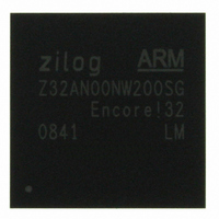
Z32AN00NW200SG Zilog, Z32AN00NW200SG Datasheet - Page 55

Z32AN00NW200SG
Manufacturer Part Number
Z32AN00NW200SG
Description
IC ARM922T MCU 200MHZ 256-BGA
Manufacturer
Zilog
Series
Encore!® 32r
Datasheet
1.Z32AN00NW200SG.pdf
(196 pages)
Specifications of Z32AN00NW200SG
Core Processor
ARM9
Core Size
16/32-Bit
Speed
200MHz
Connectivity
EBI/EMI, IrDA, SmartCard, SPI, UART/USART, USB OTG
Peripherals
DMA, LCD, Magnetic Card Reader, POR, PWM, WDT
Number Of I /o
76
Program Memory Type
ROMless
Ram Size
64K x 8
Voltage - Supply (vcc/vdd)
1.71 V ~ 3.6 V
Data Converters
A/D 4x10b
Oscillator Type
Internal
Operating Temperature
-40°C ~ 85°C
Package / Case
256-LBGA
For Use With
269-4713 - KIT DEV ENCORE 32 SERIES
Lead Free Status / RoHS Status
Lead free / RoHS Compliant
Eeprom Size
-
Program Memory Size
-
Other names
269-4717
Available stocks
Company
Part Number
Manufacturer
Quantity
Price
- Current page: 55 of 196
- Download datasheet (4Mb)
Z32AN Series Data Sheet
7.4.1.1
DS0200-003
31:25
23:22
21:20
19:18
17:16
15:08
07:06
05:04
03:00
Offset 000h: SDR_CFG – SDRAM Configuration Register
Bits
24
Type
RW
RW
RW
RW
RW
RW
RO
RO
RO
RO
Reset
00
00
00
00
11
11
9h
0
0
0
Description
Reserved
Interleave Address (INTER):
When set, bank address derived from address bits between the column (LSBs) and the
row (MSBs). See section 7.2.2.
Reserved
Row Width (ROW): Row bits. See section 7.2.2.
Reserved
Column Width (COL): Column bits. See section 7.2.2.
Reserved
Minimum PRECHARGE Delay (TRP): Minimum delay from PRECHARGE to any other
command to the same bank: The SDRAM Controller will guarantee the specified number
of SDCLK cycles between PRECHARGE and any subsequent command to the same bank.
Minimum ACTIVE Delay (TRCD): Minimum delay from ACTIVE to READ or WRITE
command. The SDRAM Controller will guarantee the specified number of SDCLK cycles
between ACTIVE and READ/WRITE commands.
Minimum AUTO_REFRESH Period (TRFC): The SDRAM Controller will guarantee
the specified number of SDCLK cycles between AUTO REFRESH commands.
00: 11 bits
01: 12 bits
10: 13 bits
11: reserved
00: 8 bits
01: 9 bits
10: 10 bits
11: 11 bits
00: 1 clock
01: 2 clocks
10: 3 clocks
11: 4 clocks
00: 1 clock
01: 2 clocks
10: 3 clocks
11: 4 clocks
0000: 1 clock
0001: 2 clocks
...
1001: 10 clocks
1010 - 1111: reserved
When cleared, bank address derived from MSBs.
Page 42
Related parts for Z32AN00NW200SG
Image
Part Number
Description
Manufacturer
Datasheet
Request
R

Part Number:
Description:
Communication Controllers, ZILOG INTELLIGENT PERIPHERAL CONTROLLER (ZIP)
Manufacturer:
Zilog, Inc.
Datasheet:

Part Number:
Description:
KIT DEV FOR Z8 ENCORE 16K TO 64K
Manufacturer:
Zilog
Datasheet:

Part Number:
Description:
KIT DEV Z8 ENCORE XP 28-PIN
Manufacturer:
Zilog
Datasheet:

Part Number:
Description:
DEV KIT FOR Z8 ENCORE 8K/4K
Manufacturer:
Zilog
Datasheet:

Part Number:
Description:
KIT DEV Z8 ENCORE XP 28-PIN
Manufacturer:
Zilog
Datasheet:

Part Number:
Description:
DEV KIT FOR Z8 ENCORE 4K TO 8K
Manufacturer:
Zilog
Datasheet:

Part Number:
Description:
CMOS Z8 microcontroller. ROM 16 Kbytes, RAM 256 bytes, speed 16 MHz, 32 lines I/O, 3.0V to 5.5V
Manufacturer:
Zilog, Inc.
Datasheet:

Part Number:
Description:
Low-cost microcontroller. 512 bytes ROM, 61 bytes RAM, 8 MHz
Manufacturer:
Zilog, Inc.
Datasheet:

Part Number:
Description:
Z8 4K OTP Microcontroller
Manufacturer:
Zilog, Inc.
Datasheet:

Part Number:
Description:
CMOS SUPER8 ROMLESS MCU
Manufacturer:
Zilog, Inc.
Datasheet:

Part Number:
Description:
SL1866 CMOSZ8 OTP Microcontroller
Manufacturer:
Zilog, Inc.
Datasheet:

Part Number:
Description:
SL1866 CMOSZ8 OTP Microcontroller
Manufacturer:
Zilog, Inc.
Datasheet:

Part Number:
Description:
OTP (KB) = 1, RAM = 125, Speed = 12, I/O = 14, 8-bit Timers = 2, Comm Interfaces Other Features = Por, LV Protect, Voltage = 4.5-5.5V
Manufacturer:
Zilog, Inc.
Datasheet:

Part Number:
Description:
Manufacturer:
Zilog, Inc.
Datasheet:


