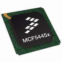
MCF54455CVR200 Freescale Semiconductor, MCF54455CVR200 Datasheet - Page 14

MCF54455CVR200
Manufacturer Part Number
MCF54455CVR200
Description
IC MPU 32BIT 200MHZ 360TEPBGA
Manufacturer
Freescale Semiconductor
Series
MCF5445xr
Datasheet
1.MCF54452CVR200.pdf
(48 pages)
Specifications of MCF54455CVR200
Core Processor
Coldfire V4
Core Size
32-Bit
Speed
200MHz
Connectivity
I²C, SPI, SSI, UART/USART, USB OTG
Peripherals
DMA, WDT
Number Of I /o
132
Program Memory Type
ROMless
Ram Size
32K x 8
Voltage - Supply (vcc/vdd)
1.35 V ~ 3.6 V
Oscillator Type
Internal
Operating Temperature
-40°C ~ 85°C
Package / Case
360-TEPBGA
Processor Series
MCF544x
Core
ColdFire V4
Data Bus Width
32 bit
Program Memory Size
16 KB
Data Ram Size
32 KB
Interface Type
I2C, SPI, SSI
Maximum Clock Frequency
66 MHz
Number Of Timers
8
Operating Supply Voltage
- 0.3 V to + 4 V
Maximum Operating Temperature
+ 85 C
Mounting Style
SMD/SMT
3rd Party Development Tools
JLINK-CF-BDM26, EWCF
Development Tools By Supplier
M54455EVB
Minimum Operating Temperature
- 40 C
On-chip Adc
16 bit, 16 Channel
On-chip Dac
16 bit, 16 Channel
Leaded Process Compatible
Yes
Rohs Compliant
Yes
Peak Reflow Compatible (260 C)
Yes
For Use With
M54455EVB - BOARD EVAL FOR MCF5445X
Lead Free Status / RoHS Status
Lead free / RoHS Compliant
Eeprom Size
-
Program Memory Size
-
Data Converters
-
Lead Free Status / Rohs Status
Lead free / RoHS Compliant
Available stocks
Company
Part Number
Manufacturer
Quantity
Price
Company:
Part Number:
MCF54455CVR200
Manufacturer:
Freescale Semiconductor
Quantity:
135
Company:
Part Number:
MCF54455CVR200
Manufacturer:
FREESCAL
Quantity:
624
1
2
3
4
5
6
7
8
9
Pull-ups are generally only enabled on pins with their primary function, except as noted.
Refers to pin’s primary function.
Enabled only in oscillator bypass mode (internal crystal oscillator is disabled).
Serial boot must select 0-bit boot port size to enable the GPIO mode on these pins.
When the PCI is enabled, all PCI bus pins come up configured as such. This includes the PCI_GNT and PCI_REQ lines, which have
GPIO. The IRQ1/PCI_INTA signal is a special case. It comes up as PCI_INTA when booting as a PCI agent and as GPIO when booting
as a PCI host.
For the 360 TEPBGA, booting with PCI disabled results in all dedicated PCI pins being safe-stated. The PCI_GNT and PCI_REQ lines
and IRQ1/PCI_INTA come up as GPIO.
GPIO functionality is determined by the edge port module. The pin multiplexing and control module is only responsible for assigning
the alternate functions.
Depends on programmed polarity of the USB_VBUS_OC signal.
Pull-up when the serial boot facility (SBF) controls the pin
If JTAG_EN is asserted, these pins default to Alternate 1 (JTAG) functionality. The pin multiplexing and control module is not
responsible for assigning these pins.
Pin Assignments and Reset States
14
Signal Name
VDD_A_PLL
VDD_OSC
VDD_RTC
VSS_OSC
SD_VDD
EVDD
IVDD
VSS
GPIO
Table 4. MCF5445x Signal Information and Muxing (continued)
—
—
—
—
—
—
—
—
MCF5445x ColdFire
Alternate 1
—
—
—
—
—
—
—
—
®
Power Supplies
Microprocessor Data Sheet, Rev. 6
Alternate 2
—
—
—
—
—
—
—
—
—
—
—
—
—
—
—
—
—
—
—
—
—
—
—
—
—
—
—
—
—
—
—
—
256 MAPBGA
G5, G12, H5, H12,
J6–11, K6–11, T1,
J5, J12, K5, K12,
L7–11, M9, M10
A1, A16, F6–11,
E6–12, F5, F12
G6–11, H6–11,
MCF54450
MCF54451
Freescale Semiconductor
L5–6, L12
M12
K15
T16
L14
L15
G11, G14, G16, J7,
J16, L7, L16, N16,
J9–14, K7, K9–14,
A1, A22, B14, G7,
360 TEPBGA
P7, R16, T8, T12,
T9–11, T13, T15,
D6, D8, D14, F4,
H4, N4, R4, W4,
G9–10, G12–13,
K16, L9–14, M7,
F19, H19, K19,
M19, R19, U19
M9–M14, M16,
N9–14, P9–14,
W7, W8, W12,
D13, D19, G8,
G15, H7, H16,
MCF54452
MCF54453
MCF54454
MCF54455
P16, R7, T7,
AB1, AB22
W16, W19
T14, T16
C14
C13
C16
B16


