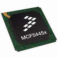
MCF54455CVR200 Freescale Semiconductor, MCF54455CVR200 Datasheet - Page 20

MCF54455CVR200
Manufacturer Part Number
MCF54455CVR200
Description
IC MPU 32BIT 200MHZ 360TEPBGA
Manufacturer
Freescale Semiconductor
Series
MCF5445xr
Datasheet
1.MCF54452CVR200.pdf
(48 pages)
Specifications of MCF54455CVR200
Core Processor
Coldfire V4
Core Size
32-Bit
Speed
200MHz
Connectivity
I²C, SPI, SSI, UART/USART, USB OTG
Peripherals
DMA, WDT
Number Of I /o
132
Program Memory Type
ROMless
Ram Size
32K x 8
Voltage - Supply (vcc/vdd)
1.35 V ~ 3.6 V
Oscillator Type
Internal
Operating Temperature
-40°C ~ 85°C
Package / Case
360-TEPBGA
Processor Series
MCF544x
Core
ColdFire V4
Data Bus Width
32 bit
Program Memory Size
16 KB
Data Ram Size
32 KB
Interface Type
I2C, SPI, SSI
Maximum Clock Frequency
66 MHz
Number Of Timers
8
Operating Supply Voltage
- 0.3 V to + 4 V
Maximum Operating Temperature
+ 85 C
Mounting Style
SMD/SMT
3rd Party Development Tools
JLINK-CF-BDM26, EWCF
Development Tools By Supplier
M54455EVB
Minimum Operating Temperature
- 40 C
On-chip Adc
16 bit, 16 Channel
On-chip Dac
16 bit, 16 Channel
Leaded Process Compatible
Yes
Rohs Compliant
Yes
Peak Reflow Compatible (260 C)
Yes
For Use With
M54455EVB - BOARD EVAL FOR MCF5445X
Lead Free Status / RoHS Status
Lead free / RoHS Compliant
Eeprom Size
-
Program Memory Size
-
Data Converters
-
Lead Free Status / Rohs Status
Lead free / RoHS Compliant
Available stocks
Company
Part Number
Manufacturer
Quantity
Price
Company:
Part Number:
MCF54455CVR200
Manufacturer:
Freescale Semiconductor
Quantity:
135
Company:
Part Number:
MCF54455CVR200
Manufacturer:
FREESCAL
Quantity:
624
Electrical Characteristics
5.5
The clock module configures the device for one of several clocking methods. Clocking modes include internal phase-locked
loop (PLL) clocking with an external clock reference or an external crystal reference supported by an internal crystal amplifier.
The PLL can also be disabled, and an external oscillator can directly clock the device.
The specifications in
specification is based on an acceptable tolerance for the PLL, which yields 50% duty-cycle internal clocks to all on-chip
peripherals. The MCF5445x devices use the input clock signal as its synchronous bus clock for PCI. A poor duty cycle on the
input clock, may affect the overall timing margin to external devices. If negative edge logic is used to interface to PCI, providing
a 50% duty-cycle input clock aids in simplifying overall system design.
20
1
2
3
4
5
6
7
Weak Internal Pull Up Device Current, tested at V
Input Capacitance
Load Capacitance
DC Injection Current
IV
specification for an example circuit. There are three PV
PV
Worst-case tristate leakage current with only one I/O pin high. Since all I/Os share power when high, the leakage current
is distributed among them. With all I/Os high, this spec reduces to ±2 μA min/max.
Refer to the MCF54455 Reference Manual signals description chapter for pins having weak internal pull-up devices.
This parameter is characterized before qualification rather than 100% tested.
All functional non-supply pins are internally clamped to V
Input must be current limited to the value specified. To determine the value of the required current-limiting resistor,
calculate resistance values for positive and negative clamp voltages, then use the larger of the two values.
Power supply must maintain regulation within operating V
current conditions. If positive injection current (V
and could result in external power supply going out of regulation. Ensure the external V
than the maximum injection current. This is the greatest risk when the MCU is not consuming power. Examples are: if
no system clock is present, or if clock rate is very low which would reduce overall power consumption. Also, at power-up,
the system clock is not present during the power-up sequence until the PLL has attained lock.
All input-only pins
All input/output (three-state) pins
High drive strength
Single Pin Limit
Total MCU Limit, Includes sum of all stressed pins
Low drive strength
DD
DD
V
and PV
NEGCLAMP
ClockTiming Specifications
input.
Item
C1
DD
Table 9
should be at the same voltage. PV
=V
4
Cycle time
SS
3, 5, 6, 7
– 0.3 V, V
are for the CLKIN input pin (EXTAL input driven by an external clock reference). The duty cycle
Characteristic
MCF5445x ColdFire
POSCLAMP
Table 9. Input Clock Timing Requirements
Specification
Table 8. DC Electrical Specifications
= V
DD
IL
in
®
+ 0.3
Max.
> V
DD
Microprocessor Data Sheet, Rev. 6
should have a filtered input. Please see the PLL section of this
DD
3
DD
) is greater than I
SS
DD
inputs, one for each PLL. A filter circuit should used on each
and their respective V
range during instantaneous and operating maximum
Symbol
I
APU
C
C
I
Min
DD
IC
15
in
L
, the injection current may flow out of V
DD
.
Max
Min
-1.0
40
–10
DD
-10
—
—
load shunts current greater
Freescale Semiconductor
Unit
ns
–130
Max
1.0
25
50
10
7
7
Units
mA
μA
pF
pF
DD


