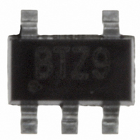
EL8103IWZ-T7A Intersil, EL8103IWZ-T7A Datasheet - Page 10

EL8103IWZ-T7A
Manufacturer Part Number
EL8103IWZ-T7A
Description
IC OPAMP 500MHZ R-R SOT23-5
Manufacturer
Intersil
Datasheet
1.EL8103IWZ-T7A.pdf
(14 pages)
Specifications of EL8103IWZ-T7A
Amplifier Type
Voltage Feedback
Number Of Circuits
1
Output Type
Rail-to-Rail
Slew Rate
600 V/µs
Gain Bandwidth Product
200MHz
-3db Bandwidth
500MHz
Current - Input Bias
6µA
Voltage - Input Offset
800µV
Current - Supply
5.6mA
Current - Output / Channel
65mA
Voltage - Supply, Single/dual (±)
3 V ~ 5 V, ±1.5 V ~ 2.5 V
Operating Temperature
-40°C ~ 85°C
Mounting Type
Surface Mount
Package / Case
SOT-23-5, SC-74A, SOT-25
Lead Free Status / RoHS Status
Lead free / RoHS Compliant
Other names
EL8103IWZ-T7A
EL8103IWZ-T7ATR
EL8103IWZ-T7ATR
Available stocks
Company
Part Number
Manufacturer
Quantity
Price
Company:
Part Number:
EL8103IWZ-T7A
Manufacturer:
Intersil
Quantity:
500
Part Number:
EL8103IWZ-T7A
Manufacturer:
INTERSIL
Quantity:
20 000
output to eliminate most peaking. However, this will reduce
the gain slightly. If the gain setting is greater than 1, the gain
resistor R
which may be created by the additional series resistor at the
output.
When used as a cable driver, double termination is always
recommended for reflection-free performance. For those
applications, a back-termination series resistor at the
amplifier’s output will isolate the amplifier from the cable and
allow extensive capacitive drive. However, other applications
may have high capacitive loads without a back-termination
resistor. Again, a small series resistor at the output can help
to reduce peaking.
Disable/Power-Down
The EL8102 can be disabled and its output placed in a high
impedance state. The turn-off time is about 25ns and the
turn-on time is about 200ns. When disabled, the amplifier’s
supply current is reduced to 30µA typically, thereby
effectively eliminating the power consumption. The
amplifier’s power down can be controlled by standard TTL or
CMOS signal levels at the ENABLE pin. The applied logic
signal is relative to V
applying a signal that is less than 0.8V above V
the amplifier. The amplifier will be disabled when the signal
at ENABLE pin is 2V above V
Output Drive Capability
The EL8102, EL8103 do not have internal short circuit
protection circuitry. They have a typical short circuit current
of 80mA sourcing and 150mA sinking for the output is
connected to half way between the rails with a 10Ω resistor.
If the output is shorted indefinitely, the power dissipation
could easily increase such that the part will be destroyed.
Maximum reliability is maintained if the output current never
exceeds ±40mA. This limit is set by the design of the internal
metal interconnections.
Power Dissipation
With the high output drive capability of the EL8102, EL8103,
It is possible to exceed the +125°C absolute maximum
junction temperature under certain load current conditions.
Therefore, it is important to calculate the maximum junction
temperature for the application to determine if the load
conditions or package types need to be modified for the
amplifier to remain in the safe operating area.
The maximum power dissipation allowed in a package is
determined according to Equation 2:
PD
MAX
=
G
T
-------------------------------------------- -
can then be chosen to make up for any gain loss
JMAX
θ
–
JA
T
AMAX
S
- pin. Letting the ENABLE pin float or
10
S
-.
S
- will enable
EL8102, EL8103
(EQ. 2)
Where:
The maximum power dissipation actually produced by an IC
is the total quiescent supply current times the total power
supply voltage, plus the power in the IC due to the load, or:
For sourcing, Equation 3:
For sinking, Equation 4:
PD
Where:
By setting the two PD
can solve the output current and R
overheat.
Power Supply Bypassing and Printed Circuit
Board Layout
As with any high frequency device, a good printed circuit
board layout is necessary for optimum performance. Lead
lengths should be as short as possible. The power supply
pin must be well bypassed to reduce the risk of oscillation.
For normal single supply operation, where the V
connected to the ground plane, a single 4.7µF tantalum
capacitor in parallel with a 0.1µF ceramic capacitor from V
to GND will suffice. This same capacitor combination should
be placed at each supply pin to ground if split supplies are to
be used. In this case, the VS- pin becomes the negative
supply rail.
For good AC performance, parasitic capacitance should be
kept to a minimum. Use of wire wound resistors should be
avoided because of their additional series inductance. Use
of sockets should also be avoided if possible. Sockets add
parasitic inductance and capacitance that can result in
compromised performance. Minimizing parasitic capacitance
at the amplifier’s inverting input pin is very important. The
feedback resistor should be placed very close to the
inverting input pin. Strip line design techniques are
recommended for the signal traces.
PD
T
T
θ
MAX
V
I
V
R
I
MAX
SMAX
LOAD
JA
AMAX
JMAX
S
OUT
LOAD
= Total supply voltage
= Thermal resistance of the package
=
=
= Maximum output voltage of the application
= Load current
= Maximum quiescent supply current
= Maximum junction temperature
= Maximum ambient temperature
V
= Load resistance tied to ground
V
S
S
×
×
I
I
SMAX
SMAX
+
MAX
+
(
(
V
V
OUT
S
equations equal to each other, we
–
V
–
OUT
V
S
-
)
LOAD
) I
×
×
V
--------------- -
LOAD
OUT
R
to avoid the device
L
S
August 10, 2007
- pin is
FN7104.7
(EQ. 3)
(EQ. 4)
S
+


