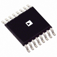
AD8370AREZ Analog Devices Inc, AD8370AREZ Datasheet - Page 13

AD8370AREZ
Manufacturer Part Number
AD8370AREZ
Description
IC AMP VGA DIFF LN 16TSSOP
Manufacturer
Analog Devices Inc
Type
Var Gain Ampr
Datasheet
1.AD8370AREZ-RL7.pdf
(28 pages)
Specifications of AD8370AREZ
Amplifier Type
Variable Gain
Number Of Circuits
1
Output Type
Differential
Slew Rate
5750 V/ns
-3db Bandwidth
750MHz
Current - Input Bias
400pA
Current - Supply
79mA
Voltage - Supply, Single/dual (±)
3 V ~ 5.5 V
Operating Temperature
-40°C ~ 85°C
Mounting Type
Surface Mount
Package / Case
16-TSSOP Exposed Pad, 16-eTSSOP, 16-HTSSOP
No. Of Amplifiers
1
Bandwidth
750MHz
No. Of Channels
1
Supply Voltage Range
3V To 5.5V
Amplifier Case Style
TSSOP
No. Of Pins
16
Operating Temperature Range
-40°C To +85°C
Number Of Channels
1
Number Of Elements
2
Power Supply Requirement
Single
Common Mode Rejection Ratio
77dB
Voltage Gain Db
34dB
Input Resistance
0.0002@5VMohm
Input Bias Current
0.9@5VnA
Single Supply Voltage (typ)
5V
Dual Supply Voltage (typ)
Not RequiredV
Power Dissipation
575mW
Rail/rail I/o Type
No
Single Supply Voltage (min)
3V
Single Supply Voltage (max)
5.5V
Dual Supply Voltage (min)
Not RequiredV
Dual Supply Voltage (max)
Not RequiredV
Operating Temp Range
-40C to 85C
Operating Temperature Classification
Industrial
Mounting
Surface Mount
Pin Count
16
Package Type
TSSOP EP
Lead Free Status / RoHS Status
Lead free / RoHS Compliant
Current - Output / Channel
-
Gain Bandwidth Product
-
Voltage - Input Offset
-
Lead Free Status / Rohs Status
Compliant
Available stocks
Company
Part Number
Manufacturer
Quantity
Price
Company:
Part Number:
AD8370AREZ
Manufacturer:
ADI
Quantity:
1 636
Part Number:
AD8370AREZ
Manufacturer:
ADI/亚德诺
Quantity:
20 000
Part Number:
AD8370AREZ-REEL7
Manufacturer:
ADI/亚德诺
Quantity:
20 000
Company:
Part Number:
AD8370AREZ-RL7
Manufacturer:
AD
Quantity:
735
Part Number:
AD8370AREZ-RL7
Manufacturer:
ADI/亚德诺
Quantity:
20 000
THEORY OF OPERATION
The AD8370 is a low cost, digitally controlled, fine adjustment
variable gain amplifier (VGA) that provides both high IP3 and
low noise figure. The AD8370 is fabricated on an ADI
proprietary high performance 25 GHz silicon bipolar process.
The –3 dB bandwidth is approximately 750 MHz throughout
the variable gain range. The typical quiescent current of the
AD8370 is 78 mA. A power-down feature reduces the current to
less than 4 mA. The input impedance is approximately 200 Ω
differential, and the output impedance is approximately 100 Ω
differential to be compatible with saw filters and matching
networks used in intermediate frequency (IF) radio
applications. Because there is no feedback between the input
and output and stages within the amplifier, the input amplifier
is isolated from variations in output loading and from
subsequent impedance changes, and excellent input to output
isolation is realized. Excellent distortion performance and wide
bandwidth make the AD8370 a suitable gain control device for
modern differential receiver designs. The AD8370 differential
input and output configuration is ideally suited to fully
differential signal chain circuit designs, although it can be
adapted to single-ended system applications, if required.
BLOCK ARCHITECTURE
The three basic building blocks of the AD8370 are a high/low
gain selectable input preamplifier, a digitally controlled
transconductance (g
PREAMPLIFIER
There are two selectable input preamplifiers. Selection is made
by the most significant bit (MSB) of the serial gain control data-
word. In the high gain mode, the overall device gain is 7.1 V/V
(17 dB) above the low gain setting. The two preamplifiers give
the AD8370 the ability to accommodate a wide range of input
amplitudes. The overlap between the two gain ranges allows the
user some flexibility based on noise and distortion demands.
See the Choosing Between Gain Ranges section for more
information.
PWUP
ICOM
ICOM
INLO
INHI
16
15
4
2
1
VCCI
3
PRE
AMP
Figure 37. Functional Block Diagram
m
) block, and a fixed gain output stage.
TRANSCONDUCTANCE
DATA CLCK LTCH
14
SHIFT REGISTER
AND LATCHES
BIAS CELL
13
12
VCCO
11
OUTPUT
AMP
AD8370
VCCO
6
10
5
7
8
9
VOCM
OCOM
OPHI
OPLO
OCOM
Rev. A | Page 13 of 28
The input impedance is approximately 200 Ω differential,
regardless of which preamplifier is selected. Note that the input
impedance is formed by using active circuit elements and is not
set by passive components. See Figure 38 for a simplified
schematic of the input interface.
TRANSCONDUCTANCE STAGE
The digitally controlled g
gain and makes gain adjustments within each gain range. The
step size resolution ranges from a fine ~ 0.07 dB up to a coarse
6 dB per bit, depending on the gain code. As shown in Figure 39, of
the 42 dB total range, 28 dB has resolution of better than 2 dB,
and 22 dB has resolution of better than 1 dB.
Figure 39 shows typical input levels that can be applied to this
amplifier at different gain settings. The maximum input was
determined by finding the 1 dB compression or expansion point
of the V
way, the change in the input impedance of the device is also
taken into account.
3.2
2.8
2.4
2.0
1.6
1.2
0.8
0.4
0
0
OUT
INHI/INLO
34dB
GAIN
/V
Figure 39. Gain Resolution and Nominal Input and
<0.5dB
17dB
GAIN
0.2
SOURCE
RES
Figure 38. INHI/INLO Simplified Schematic
12dB
GAIN
Output Range over the Gain Range
0.4
<1dB
6dB
GAIN
RES
gain. Note that this is not V
–8dB GAIN
<2dB
RES
0.6
V
m
SOURCE
section has 42 dB of controllable
HIGH GAIN
0.8
[V peak] (V)
0.1dB GAIN
–5dB GAIN
1.0
–11dB GAIN
–25dB GAIN
1mA
1mA
1.2
RESOLUTION
LOW GAIN
1.4
<0.5dB
2kΩ
<1dB
<2dB
RES
RES
OUT
1.6
/V
VCC/2
AD8370
IN
. In this
1.8


