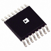
AD8370AREZ Analog Devices Inc, AD8370AREZ Datasheet - Page 16

AD8370AREZ
Manufacturer Part Number
AD8370AREZ
Description
IC AMP VGA DIFF LN 16TSSOP
Manufacturer
Analog Devices Inc
Type
Var Gain Ampr
Datasheet
1.AD8370AREZ-RL7.pdf
(28 pages)
Specifications of AD8370AREZ
Amplifier Type
Variable Gain
Number Of Circuits
1
Output Type
Differential
Slew Rate
5750 V/ns
-3db Bandwidth
750MHz
Current - Input Bias
400pA
Current - Supply
79mA
Voltage - Supply, Single/dual (±)
3 V ~ 5.5 V
Operating Temperature
-40°C ~ 85°C
Mounting Type
Surface Mount
Package / Case
16-TSSOP Exposed Pad, 16-eTSSOP, 16-HTSSOP
No. Of Amplifiers
1
Bandwidth
750MHz
No. Of Channels
1
Supply Voltage Range
3V To 5.5V
Amplifier Case Style
TSSOP
No. Of Pins
16
Operating Temperature Range
-40°C To +85°C
Number Of Channels
1
Number Of Elements
2
Power Supply Requirement
Single
Common Mode Rejection Ratio
77dB
Voltage Gain Db
34dB
Input Resistance
0.0002@5VMohm
Input Bias Current
0.9@5VnA
Single Supply Voltage (typ)
5V
Dual Supply Voltage (typ)
Not RequiredV
Power Dissipation
575mW
Rail/rail I/o Type
No
Single Supply Voltage (min)
3V
Single Supply Voltage (max)
5.5V
Dual Supply Voltage (min)
Not RequiredV
Dual Supply Voltage (max)
Not RequiredV
Operating Temp Range
-40C to 85C
Operating Temperature Classification
Industrial
Mounting
Surface Mount
Pin Count
16
Package Type
TSSOP EP
Lead Free Status / RoHS Status
Lead free / RoHS Compliant
Current - Output / Channel
-
Gain Bandwidth Product
-
Voltage - Input Offset
-
Lead Free Status / Rohs Status
Compliant
Available stocks
Company
Part Number
Manufacturer
Quantity
Price
Company:
Part Number:
AD8370AREZ
Manufacturer:
ADI
Quantity:
1 636
Part Number:
AD8370AREZ
Manufacturer:
ADI/亚德诺
Quantity:
20 000
Part Number:
AD8370AREZ-REEL7
Manufacturer:
ADI/亚德诺
Quantity:
20 000
Company:
Part Number:
AD8370AREZ-RL7
Manufacturer:
AD
Quantity:
735
Part Number:
AD8370AREZ-RL7
Manufacturer:
ADI/亚德诺
Quantity:
20 000
AD8370
CHOOSING BETWEEN GAIN RANGES
There is some overlap between the two gain ranges; users can
choose which one is most appropriate for their needs. When
deciding which preamp to use, consider resolution, noise,
linearity, and spurious-free dynamic range (SFDR). The most
important points to keep in mind are
•
•
•
•
Figure 45 provides a summary of noise, OIP3, IIP3, and SFDR
as a function of device power gain. SFDR is defined as
where:
IIP3 is the input third-order intercept point, the output
intercept point in dBm minus the gain in dB.
NF is the noise figure in dB.
N
300°K (27°C).
In general, N
temperature in degrees Kelvin, and B is the noise bandwidth in
Hertz.
As the gain increases, the input amplitude required to deliver
the same output amplitude is reduced. This results in less
distortion at the input stage, and therefore the OIP3 increases.
At some point, the distortion of the input stage becomes small
enough such that the nonlinearity of the output stage becomes
dominant. The OIP3 does not improve significantly because the
S
is source resistor noise, –174 dBm for a 1 Hz bandwidth at
–10
–20
–30
The low gain range has better gain resolution.
The high gain range has a better noise figure.
The high gain range has better linearity and SFDR at
higher gains.
Conversely, the low gain range has higher SFDR at lower
gains.
SFDR
50
40
30
20
10
0
–30
IIP3 LOW GAIN
Figure 45. OIP3, IIP3, NF, and SFDR Variation with Gain
SFDR LOW GAIN
=
S
2
3
–20
= 10 log
(
IIP3
NF LOW GAIN
−
–10
NF
10
(kTB), where k = 1.374 ×10
POWER GAIN (dB)
OIP3 LOW GAIN
−
N
0
S
)
NF HIGH GAIN
10
SFDR HIGH GAIN
20
OIP3 HIGH GAIN
IIP3 HIGH GAIN
30
−23
, T is the
40
180
170
160
150
140
130
120
110
100
Rev. A | Page 16 of 28
gain is increased beyond this point, which explains the knee in
the OIP3 curve. The IIP3 curve has a knee for the same reason;
however, as the gain is increased beyond the knee, the IIP3
starts to decrease rather than increase. This is because in this
region OIP3 is constant, therefore the higher the gain, the lower
the IIP3. The two gain ranges have equal SFDR at
approximately 13 dB power gain.
LAYOUT AND OPERATING CONSIDERATIONS
Each input and output pin of the AD8370 presents either a
100 Ω or 50 Ω impedance relative to their respective ac grounds.
To ensure that signal integrity is not seriously impaired by the
printed circuit board, the relevant connection traces should
provide an appropriate characteristic impedance to the ground
plane. This can be achieved through proper layout.
When laying out an RF trace with a controlled impedance,
consider the following:
•
•
•
Keep the length of the input and output connection lines as
short as possible.
Figure 46 shows the cross section of a PC board, and Table 5
show the dimensions that provide a 100 Ω line impedance for
FR-4 board material with εr = 4.6.
Table 5.
W
H
T
It possible to approximate a 100 Ω trace on a board designed
with the 50 Ω dimensions above by removing the ground plane
within 3 line-widths of the area directly below the trace.
H
Space the ground plane to either side of the signal trace at
least three line-widths away to ensure that a microstrip
(vertical dielectric) line is formed, rather than a coplanar
(lateral dielectric) waveguide.
Ensure that the width of the microstrip line is constant and
that there are as few discontinuities as possible, such as
component pads, along the length of the line. Width
variations cause impedance discontinuities in the line and
may result in unwanted reflections.
Do not use silkscreen over the signal line because it alters
the line impedance.
E
R
Figure 46. Cross-Sectional View of a PC Board
100 Ω
22 mils
53 mils
2 mils
3W
W
3W
50 Ω
13 mils
8 mils
2 mils
T


