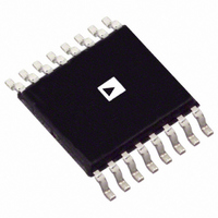
AD8370AREZ Analog Devices Inc, AD8370AREZ Datasheet - Page 17

AD8370AREZ
Manufacturer Part Number
AD8370AREZ
Description
IC AMP VGA DIFF LN 16TSSOP
Manufacturer
Analog Devices Inc
Type
Var Gain Ampr
Datasheet
1.AD8370AREZ-RL7.pdf
(28 pages)
Specifications of AD8370AREZ
Amplifier Type
Variable Gain
Number Of Circuits
1
Output Type
Differential
Slew Rate
5750 V/ns
-3db Bandwidth
750MHz
Current - Input Bias
400pA
Current - Supply
79mA
Voltage - Supply, Single/dual (±)
3 V ~ 5.5 V
Operating Temperature
-40°C ~ 85°C
Mounting Type
Surface Mount
Package / Case
16-TSSOP Exposed Pad, 16-eTSSOP, 16-HTSSOP
No. Of Amplifiers
1
Bandwidth
750MHz
No. Of Channels
1
Supply Voltage Range
3V To 5.5V
Amplifier Case Style
TSSOP
No. Of Pins
16
Operating Temperature Range
-40°C To +85°C
Number Of Channels
1
Number Of Elements
2
Power Supply Requirement
Single
Common Mode Rejection Ratio
77dB
Voltage Gain Db
34dB
Input Resistance
0.0002@5VMohm
Input Bias Current
0.9@5VnA
Single Supply Voltage (typ)
5V
Dual Supply Voltage (typ)
Not RequiredV
Power Dissipation
575mW
Rail/rail I/o Type
No
Single Supply Voltage (min)
3V
Single Supply Voltage (max)
5.5V
Dual Supply Voltage (min)
Not RequiredV
Dual Supply Voltage (max)
Not RequiredV
Operating Temp Range
-40C to 85C
Operating Temperature Classification
Industrial
Mounting
Surface Mount
Pin Count
16
Package Type
TSSOP EP
Lead Free Status / RoHS Status
Lead free / RoHS Compliant
Current - Output / Channel
-
Gain Bandwidth Product
-
Voltage - Input Offset
-
Lead Free Status / Rohs Status
Compliant
Available stocks
Company
Part Number
Manufacturer
Quantity
Price
Company:
Part Number:
AD8370AREZ
Manufacturer:
ADI
Quantity:
1 636
Part Number:
AD8370AREZ
Manufacturer:
ADI/亚德诺
Quantity:
20 000
Part Number:
AD8370AREZ-REEL7
Manufacturer:
ADI/亚德诺
Quantity:
20 000
Company:
Part Number:
AD8370AREZ-RL7
Manufacturer:
AD
Quantity:
735
Part Number:
AD8370AREZ-RL7
Manufacturer:
ADI/亚德诺
Quantity:
20 000
The AD8370 contains both digital and analog sections. Care
should be taken to ensure that the digital and analog sections
are adequately isolated on the PC board. The use of separate
ground planes for each section connected at only one point via
a ferrite bead inductor ensures that the digital pulses do not
adversely affect the analog section of the AD8370.
Due to the nature of the AD8370’s circuit design, care must be
taken to minimize parasitic capacitance on the input and output.
The AD8370 could become unstable with more than a few pF of
shunt capacitance on each input. Using resistors in series with
input pins is recommended under conditions of high source
capacitance.
High transient and noise levels on the power supply, ground,
and digital inputs can, under some circumstances, reprogram the
AD8370 to an unintended gain code. This further reinforces the
need for proper supply bypassing and decoupling. The user
should also be aware that probing the AD8370 and associated
circuitry during circuit debug may also induce the same effect.
PACKAGE CONSIDERATIONS
The package of the AD8370 is a compact, thermally enhanced
TSSOP 16-lead design. A large exposed paddle on the bottom of
the device provides both a thermal benefit and a low inductance
path to ground for the circuit. To make proper use of this pack-
aging feature, the PCB needs to make contact directly under the
device, connected to an ac/dc common ground reference with
as many vias as possible to lower the inductance and thermal
impedance.
SINGLE-ENDED-TO-DIFFERENTIAL CONVERSION
The AD8370 is primarily designed for differential signal inter-
facing. The device can be used for single-ended-to-differential
conversion simply by terminating the unused input to ground
using a capacitor as depicted in Figure 47. The ac coupling
capacitors should be selected such that their reactance is
negligible at the frequency of operation. For example, using
1 nF capacitors for C
SINGLE-
ENDED
SOURCE
SERIAL CONTROL
INTERFACE
R
S
Figure 47. Single-Ended-to-Differential Conversion
C
C
AC
AC
0.1μF
16
1
AC
AD8370
presents a capacitive reactance of
15
2
14
3
1nF
13
4
12
5
11
6
10
7
0.1μF
9
8
+V
C
C
S
AC
AC
R
L
Rev. A | Page 17 of 28
−j1.6 Ω on each input node at 100 MHz. This attenuates the
applied input voltage by 0.003 dB. If 10 pF capacitors had been
selected, the voltage delivered to the input would be reduced by
2.1 dB when operating with a 200 Ω source impedance.
Figure 48 illustrates the differential balance at the output for a
single-ended input drive for multiple gain codes. The differential
balance is better than 0.5 dB for signal frequencies less than
250 MHz. Figure 49 depicts the differential balance over the
entire gain range at 10 MHz. The balance is degraded for lower
gain settings because the finite common gain allows some of the
input signal applied to INHI to pass directly through to the
OPLO pin. At higher gain settings, the differential gain dominates
and balance is restored.
Even though the amplifier is no longer being driven in a balanced
manner, the distortion performance remains adequate for most
applications. Figure 50 illustrates the harmonic distortion
performance of the circuit in Figure 47 over the entire gain range.
Figure 49. Differential Output Balance at 10 MHz for a Single-Ended Drive vs.
Figure 48. Differential Output Balance for a Single-Ended Input Drive at
–0.5
–1.0
0.6
0.5
0.4
0.3
0.2
0.1
0.5
0
0
0
0
32
LOW GAIN MODE
Maximum Gain (R
100
Gain Code (R
64
FREQUENCY (MHz)
96
200
LOW GAIN MODE
(GAIN CODE LG127)
GAIN CODE
L
= 1 kΩ, C
HIGH GAIN MODE
(GAIN CODE HG255)
L
0
= 1 kΩ, C
300
HIGH GAIN MODE
32
AC
= 10 nF)
AC
= 10 nF)
64
400
96
AD8370
128
500


