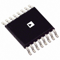
AD8370AREZ Analog Devices Inc, AD8370AREZ Datasheet - Page 15

AD8370AREZ
Manufacturer Part Number
AD8370AREZ
Description
IC AMP VGA DIFF LN 16TSSOP
Manufacturer
Analog Devices Inc
Type
Var Gain Ampr
Datasheet
1.AD8370AREZ-RL7.pdf
(28 pages)
Specifications of AD8370AREZ
Amplifier Type
Variable Gain
Number Of Circuits
1
Output Type
Differential
Slew Rate
5750 V/ns
-3db Bandwidth
750MHz
Current - Input Bias
400pA
Current - Supply
79mA
Voltage - Supply, Single/dual (±)
3 V ~ 5.5 V
Operating Temperature
-40°C ~ 85°C
Mounting Type
Surface Mount
Package / Case
16-TSSOP Exposed Pad, 16-eTSSOP, 16-HTSSOP
No. Of Amplifiers
1
Bandwidth
750MHz
No. Of Channels
1
Supply Voltage Range
3V To 5.5V
Amplifier Case Style
TSSOP
No. Of Pins
16
Operating Temperature Range
-40°C To +85°C
Number Of Channels
1
Number Of Elements
2
Power Supply Requirement
Single
Common Mode Rejection Ratio
77dB
Voltage Gain Db
34dB
Input Resistance
0.0002@5VMohm
Input Bias Current
0.9@5VnA
Single Supply Voltage (typ)
5V
Dual Supply Voltage (typ)
Not RequiredV
Power Dissipation
575mW
Rail/rail I/o Type
No
Single Supply Voltage (min)
3V
Single Supply Voltage (max)
5.5V
Dual Supply Voltage (min)
Not RequiredV
Dual Supply Voltage (max)
Not RequiredV
Operating Temp Range
-40C to 85C
Operating Temperature Classification
Industrial
Mounting
Surface Mount
Pin Count
16
Package Type
TSSOP EP
Lead Free Status / RoHS Status
Lead free / RoHS Compliant
Current - Output / Channel
-
Gain Bandwidth Product
-
Voltage - Input Offset
-
Lead Free Status / Rohs Status
Compliant
Available stocks
Company
Part Number
Manufacturer
Quantity
Price
Company:
Part Number:
AD8370AREZ
Manufacturer:
ADI
Quantity:
1 636
Part Number:
AD8370AREZ
Manufacturer:
ADI/亚德诺
Quantity:
20 000
Part Number:
AD8370AREZ-REEL7
Manufacturer:
ADI/亚德诺
Quantity:
20 000
Company:
Part Number:
AD8370AREZ-RL7
Manufacturer:
AD
Quantity:
735
Part Number:
AD8370AREZ-RL7
Manufacturer:
ADI/亚德诺
Quantity:
20 000
APPLICATIONS
BASIC CONNECTIONS
Figure 44 shows the minimum connections required for basic
operation of the AD8370. Supply voltages between 3.0 V and
5.5 V are allowed. The supply to the VCCO and VCCI pins
should be decoupled with at least one low inductance, surface-
mount ceramic capacitor of 0.1 μF placed as close as possible to
the device.
The AD8370 is designed to be used in differential signal chains.
Differential signaling allows improved even-order harmonic
cancellation and better common-mode immunity than can be
achieved using a single-ended design. To fully exploit these
benefits, it is necessary to drive and load the device in a
balanced manner. This requires some care to ensure that the
common-mode impedance values presented to each set of
inputs and outputs are balanced. Driving the device with an
unbalanced source can degrade the common-mode rejection
ratio. Loading the device with an unbalanced load can cause
degradation to even-order harmonic distortion and premature
output compression. In general, optimum designs are fully
balanced, although the AD8370 still provides impressive
performance when used in an unbalanced environment.
The AD8370 is a fine adjustment, VGA. The gain control
transfer function is linear in voltage gain. On a decibel scale,
this results in the logarithmic transfer functions shown in
Figure 4. At the low end of the gain transfer function, the slope
is steep, providing a rather coarse control function. At the high
end of the gain control range, the decibel step size decreases,
allowing precise gain adjustment.
BALANCED
SOURCE
SERIAL CONTROL
INTERFACE
R
R
2
2
S
S
100pF
1nF
1nF
0.1μF
FERRITE
Figure 44. Basic Connections
16
1
AD8370
BEAD
15
2
14
3
0.1μF
FERRITE
13
1nF
4
BEAD
12
5
11
6
10
7
100pF
9
8
+V
S
1nF
1nF
(3.0V TO 5.0V)
R
L
BALANCED
LOAD
Rev. A | Page 15 of 28
GAIN CODES
The AD8370’s two gain ranges are referred to as high gain (HG)
and low gain (LG). Within each range, there are 128 possible
gain codes. Therefore, the minimum gain in the low gain range
is given by the nomenclature LG0 whereas the maximum gain
in that range is given by LG127. The same is true for the high
gain range. Both LG0 and HG0 essentially turn off the variable
transconductance stage, and thus no output is available with
these codes (see Figure 26).
The theoretical linear voltage gain can be expressed with respect
to the gain code as
where:
For example, a gain control word of HG45 (or 10101101 binary)
results in a theoretical linear voltage gain of 17.76 V/V,
calculated as
Increments or decrements in gain within either gain range are
simply a matter of operating on the GainCode. Six –dB gain
steps, which are equivalent to doubling or halving the linear
voltage gain, are accomplished by doubling or halving the
GainCode.
When power is first applied to the AD8370, the device is
programmed to code LG0 to avoid overdriving the circuitry
following it.
POWER-UP FEATURE
The power-up feature does not affect the GainCode, and the
gain setting is preserved when in power-down mode. Powering
down the AD8370 (bringing PWUP low while power is still
applied to the device) does not erase or change the GainCode
from the AD8370, and the same gain code is in place when the
device is powered up, that is, when PWUP is brought high
again. Removing power from the device all together and
reapplying, however, reprograms to LG0.
A
GainCode is the digital gain control word minus the MSB
(the final 7 bits).
Vernier = 0.055744 V/V
PreGain = 7.079458 V/V
MSB is the most significant bit of the 8-bit gain control word.
The MSB sets the device in either high gain mode (MSB = 1)
or low gain mode (MSB = 0).
V
A
45 × 0.055744 × (1 + (7.079458 − 1) × 1)
is the linear voltage gain.
V
= GainCode Vernier (1 + (PreGain − 1) MSB)
AD8370


