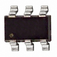
EL5108IW-T7A Intersil, EL5108IW-T7A Datasheet - Page 9

EL5108IW-T7A
Manufacturer Part Number
EL5108IW-T7A
Description
IC AMP FGA SGL 450MHZ SOT-23-6
Manufacturer
Intersil
Datasheet
1.EL5308IUZ-T7.pdf
(12 pages)
Specifications of EL5108IW-T7A
Amplifier Type
General Purpose
Number Of Circuits
1
Slew Rate
4500 V/µs
-3db Bandwidth
450MHz
Current - Input Bias
2µA
Voltage - Input Offset
3000µV
Current - Supply
3.7mA
Current - Output / Channel
135mA
Voltage - Supply, Single/dual (±)
5 V ~ 12 V, ±2.5 V ~ 6 V
Operating Temperature
-40°C ~ 85°C
Mounting Type
Surface Mount
Package / Case
SOT-23-6
Lead Free Status / RoHS Status
Contains lead / RoHS non-compliant
Output Type
-
Gain Bandwidth Product
-
Supply Voltage Range and Single-Supply
Operation
The EL5108 and EL5308 have been designed to operate
with supply voltages having a span of greater than or equal
to 5V and less than 12V. In practical terms, this means that
they will operate on dual supplies ranging from ±2.5V to ±5V.
With single-supply, they will operate from 5V to 10V.
As supply voltages continue to decrease, it becomes
necessary to provide input and output voltage ranges that
can get as close as possible to the supply voltages. The
EL5108 and EL5308 have an input range which extends to
within 2V of either supply. So, for example, on ±5V supplies,
the input range is about ±3V. The output range is also quite
large, extending to within 1V of the supply rail. On a ±5V
supply, the output is therefore capable of swinging from -4V
to +4V. Single-supply output range is larger because of the
increased negative swing due to the external pull-down
resistor to ground. Figure 24 shows an AC-coupled, gain of
+2, +5V single supply circuit configuration.
Video Performance
For good video performance, an amplifier is required to
maintain the same output impedance and the same
frequency response as DC levels are changed at the output.
This is especially difficult when driving a standard video load
of 150Ω, because of the change in output current with DC
level. Previously, good differential gain could only be
achieved by running high idle currents through the output
transistors (to reduce variations in output impedance).
Special circuitry has been incorporated in the EL5108 and
EL5308 to reduce the variation of output impedance with
current output. This results in dG and dP specifications of
0.01% and 0.01°, while driving 150Ω at a gain of 2.
0.1µF
V
IN
0.1µF
325Ω
IN+
IN-
FIGURE 23. A
1k
1k
325Ω
FIGURE 24.
+5
9
+
-
+5
V
325Ω
+
325Ω
-
= +1
4.7µF
V
OUT
EL5108, EL5308
Output Drive Capability
In spite of its low 3.5mA of supply current per amplifier, the
EL5108 and EL5308 are capable of providing a maximum of
±130mA of output current.
Driving Cables and Capacitive Loads
When used as a cable driver, double termination is always
recommended for reflection-free performance. For those
applications, the back-termination series resistor will
decouple the EL5108 and EL5308 from the cable and allow
extensive capacitive drive. However, other applications may
have high capacitive loads without a back-termination
resistor. In these applications, a small series resistor (usually
between 5Ω and 50Ω) can be placed in series with the
output to eliminate most peaking.
Current Limiting
The EL5108 and EL5308 have no internal current-limiting
circuitry. If the output is shorted, it is possible to exceed the
Absolute Maximum Rating for output current or power
dissipation, potentially resulting in the destruction of the
device.
Power Dissipation
With the high output drive capability of the EL5108 and
EL5308, it is possible to exceed the +125°C Absolute
Maximum junction temperature under certain very high load
current conditions. Generally speaking when R
about 25Ω, it is important to calculate the maximum junction
temperature (T
power supply voltages, load conditions, or package type
need to be modified for the EL5108 and EL5308 to remain in
the safe operating area. These parameters are calculated as
follows:
where:
PD
where:
PD
T
JMAX
T
θ
n = Number of amplifiers in the package
PD
the package
V
I
V
R
SMAX
MAX
MAX
JA
MAX
S
OUTMAX
L
MAX
= Load resistance
= Supply voltage
= Thermal resistance of the package
=
for each amplifier can be calculated as follows:
=
= Maximum ambient temperature
= Maximum supply current of 1A
T
2 (
= Maximum power dissipation of each amplifier in
MAX
×
= Maximum output voltage (required)
V
JMAX
+
S
(
×
θ
I
JA
SMAX
) for the application to determine if
×
n PD
×
)
+
(
MAX
V
S
- V
)
OUTMAX
)
×
L
V
--------------------------- -
falls below
August 10, 2010
OUTMAX
R
L
FN7358.7


