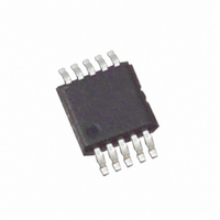
EL5421CY-T13 Intersil, EL5421CY-T13 Datasheet - Page 11

EL5421CY-T13
Manufacturer Part Number
EL5421CY-T13
Description
IC BUFFER QUAD R-R 12MHZ 10-MSOP
Manufacturer
Intersil
Datasheet
1.EL5421CYZ.pdf
(12 pages)
Specifications of EL5421CY-T13
Amplifier Type
Buffer
Number Of Circuits
4
Output Type
Rail-to-Rail
Slew Rate
10 V/µs
-3db Bandwidth
12MHz
Current - Input Bias
2nA
Voltage - Input Offset
2000µV
Current - Supply
500µA
Current - Output / Channel
120mA
Voltage - Supply, Single/dual (±)
4.5 V ~ 16.5 V, ±2.25 V ~ 8.25 V
Operating Temperature
-40°C ~ 85°C
Mounting Type
Surface Mount
Package / Case
10-MSOP, Micro10™, 10-uMAX, 10-uSOP
Lead Free Status / RoHS Status
Contains lead / RoHS non-compliant
Gain Bandwidth Product
-
Unused Buffers
It is recommended that any unused buffer have the input tied
to the ground plane.
Driving Capacitive Loads
The EL5421 can drive a wide range of capacitive loads. As
load capacitance increases, however, the -3dB bandwidth of
the device will decrease and the peaking increase. The
buffers drive 10pF loads in parallel with 10kΩ with just 1.5dB
of peaking, and 100pF with 6.4dB of peaking. If less peaking
is desired in these applications, a small series resistor
(usually between 5Ω and 50Ω) can be placed in series with
the output. However, this will obviously reduce the gain
slightly. Another method of reducing peaking is to add a
"snubber" circuit at the output. A snubber is a shunt load
consisting of a resistor in series with a capacitor. Values of
150Ω and 10nF are typical. The advantage of a snubber is
that it does not draw any DC load current or reduce the gain.
FIGURE 26. PACKAGE POWER DISSIPATION vs AMBIENT
0.6
0.5
0.4
0.3
0.2
0.1
0
0
JEDEC JESD51-3 LOW EFFECTIVE THERMAL
CONDUCTIVITY TEST BOARD
TEMPERATURE
486mW
25
AMBIENT TEMPERATURE (°C)
50
11
75
85
100
125
EL5421
Power Supply Bypassing and Printed Circuit
Board Layout
The EL5421 can provide gain at high frequency. As with any
high-frequency device, good printed circuit board layout is
necessary for optimum performance. Ground plane
construction is highly recommended, lead lengths should be
as short as possible and the power supply pins must be well
bypassed to reduce the risk of oscillation. For normal single
supply operation, where the V
a 0.1µF ceramic capacitor should be placed from V
to V
connected in parallel, placed in the region of the buffer. One
4.7µF capacitor may be used for multiple devices. This same
capacitor combination should be placed at each supply pin
to ground if split supplies are to be used.
S
- pin. A 4.7µF tantalum capacitor should then be
S
- pin is connected to ground,
August 2, 2007
S
+ to pin
FN7198.2


