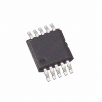
EL5421CY-T13 Intersil, EL5421CY-T13 Datasheet - Page 9

EL5421CY-T13
Manufacturer Part Number
EL5421CY-T13
Description
IC BUFFER QUAD R-R 12MHZ 10-MSOP
Manufacturer
Intersil
Datasheet
1.EL5421CYZ.pdf
(12 pages)
Specifications of EL5421CY-T13
Amplifier Type
Buffer
Number Of Circuits
4
Output Type
Rail-to-Rail
Slew Rate
10 V/µs
-3db Bandwidth
12MHz
Current - Input Bias
2nA
Voltage - Input Offset
2000µV
Current - Supply
500µA
Current - Output / Channel
120mA
Voltage - Supply, Single/dual (±)
4.5 V ~ 16.5 V, ±2.25 V ~ 8.25 V
Operating Temperature
-40°C ~ 85°C
Mounting Type
Surface Mount
Package / Case
10-MSOP, Micro10™, 10-uMAX, 10-uSOP
Lead Free Status / RoHS Status
Contains lead / RoHS non-compliant
Gain Bandwidth Product
-
Pin Descriptions
Applications Information
Product Description
The EL5421 unity gain buffer is fabricated using a high
voltage CMOS process. It exhibits rail-to-rail input and
output capability, and has low power consumption (500µA
per buffer). These features make the EL5421 ideal for a wide
range of general-purpose applications. When driving a load
of 10kΩ and 12pF, the EL5421 has a -3dB bandwidth of
12MHz and exhibits 10V/µs slew rate.
Operating Voltage, Input, and Output
The EL5421 is specified with a single nominal supply voltage
from 5V to 15V or a split supply with its total range from 5V
to 15V. Correct operation is guaranteed for a supply range of
4.5V to 16.5V. Most EL5421 specifications are stable over
both the full supply range and operating temperatures of
-40°C to +85°C. Parameter variations with operating voltage
and/or temperature are shown in the typical performance
curves.
The output swings of the EL5421 typically extend to within
80mV of positive and negative supply rails with load currents
of 5mA. Decreasing load currents will extend the output
PIN NUMBER
10
1
2
3
4
5
6
7
8
9
PIN NAME
VOUTB
VOUTC
VOUTD
VOUTA
VINA
VINB
VINC
VIND
VS+
VS-
9
Buffer A Output
Buffer A Input
Positive Power Supply
Buffer B Input
Buffer B Output
Buffer C Output
Buffer C Input
Negative Power Supply
Buffer D Input
Buffer D Output
FUNCTION
EL5421
voltage range even closer to the supply rails. Figure 23
shows the input and output waveforms for the device.
Operation is from ±5V supply with a 10kΩ load connected to
GND. The input is a 10V
approximately 9.985V
Short Circuit Current Limit
The EL5421 will limit the short circuit current to ±120mA if
the output is directly shorted to the positive or the negative
supply. If an output is shorted indefinitely, the power
FIGURE 23. OPERATION WITH RAIL-TO-RAIL INPUT AND
(Reference Circuit 1)
(Reference Circuit 2)
(Reference Circuit 2)
(Reference Circuit 1)
(Reference Circuit 2)
(Reference Circuit 1)
5V
5V
OUTPUT
P-P
EQUIVALENT CIRCUIT
P-P
.
GND
sinusoid. The output voltage is
CIRCUIT 1
CIRCUIT 2
10µs
V
T
V
A
S
IN
=±5V
=25°C
=10V
V
V
S
S
+
-
P-P
V
V
S
S
+
-
August 2, 2007
FN7198.2


