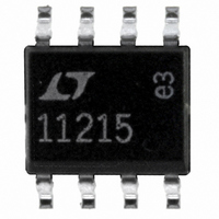
LT1121CS8-5#PBF Linear Technology, LT1121CS8-5#PBF Datasheet - Page 15

LT1121CS8-5#PBF
Manufacturer Part Number
LT1121CS8-5#PBF
Description
IC REG LDO 5V 150MA 8-SOIC
Manufacturer
Linear Technology
Specifications of LT1121CS8-5#PBF
Regulator Topology
Positive Fixed
Voltage - Output
5V
Voltage - Input
Up to 30V
Voltage - Dropout (typical)
0.42V @ 150mA
Number Of Regulators
1
Current - Output
150mA
Operating Temperature
0°C ~ 125°C
Mounting Type
Surface Mount
Package / Case
8-SOIC (3.9mm Width)
Primary Input Voltage
30V
Output Voltage Fixed
5V
Dropout Voltage Vdo
420mV
No. Of Pins
8
Output Current
150mA
Operating Temperature Range
0°C To +125°C
Msl
MSL 1 - Unlimited
Rohs Compliant
Yes
Lead Free Status / RoHS Status
Lead free / RoHS Compliant
Current - Limit (min)
-
Available stocks
Company
Part Number
Manufacturer
Quantity
Price
APPLICATIO S I FOR ATIO
applications where the ADC data outputs and control
signals are connected to a continuously active micropro-
cessor bus, it is possible to get errors in the conversion
results. These errors are due to feedthrough from the
microprocessor to the successive approximation com-
parator. The problem can be eliminated by forcing the
microprocessor into a WAIT state during conversion or by
using three-state buffers to isolate the ADC data bus. The
traces connecting the pins and bypass capacitors must be
kept short and should be made as wide as possible.
The LTC1608 has differential inputs to minimize noise
coupling. Common mode noise on the A
will be rejected by the input CMRR. The A
used as a ground sense for the A
will hold and convert the difference voltage between A
and A
be kept as short as possible. In applications where this is
not possible, the A
by side to equalize coupling.
SUPPLY BYPASSING
High quality, low series resistance ceramic, 10 F or 22 F
bypass capacitors should be used at the V
pins as shown in Figure 16 and in the Typical Application
on the first page of this data sheet. Surface mount ceramic
capacitors such as Taiyo Yuden’s LMK325BJ106MN and
LMK432BJ226MM provide excellent bypassing in a small
board space. Alternatively, 10 F tantalum capacitors in
parallel with 0.1 F ceramic capacitors can be used. By-
pass capacitors must be located as close to the pins as
possible. The traces connecting the pins and the bypass
capacitors must be kept short and should be made as wide
as possible.
IN
–
. The leads to A
CIRCUITRY
ANALOG
INPUT
IN
U
+
and A
IN
+
–
+
1
U
(Pin 1) and A
A
IN
IN
2
+
A
–
IN
–
traces should be run side
V
IN
REF
W
2.2 F
+
3
input; the LTC1608
REFCOMP
IN
IN
Figure 16. Power Supply Grounding Practice
DD
+
IN
–
22 F
4
and REFCOMP
and A
–
(Pin 2) should
input can be
AGND
U
5, 6, 7, 8
IN
–
leads
V
SS
IN
34
10 F
+
AV
LTC1608
DD
10 F
36
EXAMPLE LAYOUT
Figures 17a, 17b, 17c, 17d and 17e show the schematic
and layout of an evaluation board. The layout demon-
strates the proper use of decoupling capacitors and ground
plane with a 4-layer printed circuit board.
DC PERFORMANCE
The noise of an ADC can be evaluated in two ways: signal-
to-noise raio (SNR) in frequency domain and histogram in
time domain. The LTC1608 excels in both. Figure 19a
demonstrates that the LTC1608 has an SNR of over 90dB
in frequency domain. The noise in the time domain histo-
gram is the transition noise associated with a high resolu-
tion ADC which can be measured with a fixed DC signal
applied to the input of the ADC. The resulting output codes
are collected over a large number of conversions. The
shape of the distribution of codes will give an indication of
the magnitude of the transition noise. In Figure 18, the
distribution of output codes is shown for a DC input that
has been digitized 4096 times. The distribution is Gaussian
and the RMS code transition noise is about 0.66LSB. This
corresponds to a noise level of 90.9dB relative to full scale.
Adding to that the theoretical 98dB of quantization error
for 16-bit ADC, the resultant corresponds to an SNR level
of 90.1dB which correlates very well to the frequency
domain measurements in Dynamic Performance section.
DYNAMIC PERFORMANCE
The LTC1608 has excellent high speed sampling capabil-
ity. Fast fourier transform (FFT) test techniques are used
to test the ADC’s frequency response, distortions and
AV
DD
10 F
35
DV
DD
10 F
9
DGND
10
OV
DD
10 F
29
OGND
28
1608 F16
SYSTEM
DIGITAL
LTC1608
15


