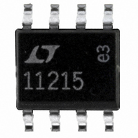
LT1121CS8-5#PBF Linear Technology, LT1121CS8-5#PBF Datasheet - Page 4

LT1121CS8-5#PBF
Manufacturer Part Number
LT1121CS8-5#PBF
Description
IC REG LDO 5V 150MA 8-SOIC
Manufacturer
Linear Technology
Specifications of LT1121CS8-5#PBF
Regulator Topology
Positive Fixed
Voltage - Output
5V
Voltage - Input
Up to 30V
Voltage - Dropout (typical)
0.42V @ 150mA
Number Of Regulators
1
Current - Output
150mA
Operating Temperature
0°C ~ 125°C
Mounting Type
Surface Mount
Package / Case
8-SOIC (3.9mm Width)
Primary Input Voltage
30V
Output Voltage Fixed
5V
Dropout Voltage Vdo
420mV
No. Of Pins
8
Output Current
150mA
Operating Temperature Range
0°C To +125°C
Msl
MSL 1 - Unlimited
Rohs Compliant
Yes
Lead Free Status / RoHS Status
Lead free / RoHS Compliant
Current - Limit (min)
-
Available stocks
Company
Part Number
Manufacturer
Quantity
Price
POWER REQUIRE E TS
LTC1608
otherwise specifications are at T
SYMBOL
V
V
I
I
P
otherwise specifications are at T
SYMBOL
f
t
t
t
t
t
t
t
t
t
t
t
t
t
t
t
t
t
Note 1: Absolute Maximum Ratings are those values beyond which the life
of a device may be impaired.
Note 2: All voltage values are with respect to ground with DGND, OGND
and AGND wired together unless otherwise noted.
TI I G CHARACTERISTICS
4
DD
SS
SMPL(MAX)
CONV
ACQ
ACQ+CONV(MIN)
1
2
3
4
5
6
7
8
9
10
11
12
13
14
DD
SS
D
W
U
PARAMETER
Positive Supply Voltage
Negative Supply Voltage
Positive Supply Current
Negative Supply Current
Power Dissipation
PARAMETER
Maximum Sampling Frequency
Conversion Time
Acquisition Time
Throughput Time (Acquisition + Conversion)
CS to RD Setup Time
CS to CONVST Setup Time
SHDN to CS Setup Time
SHDN to CONVST Wake-Up Time
CONVST Low Time
CONVST to BUSY Delay
Data Ready Before BUSY
Delay Between Conversions
Wait Time RD After BUSY
Data Access Time After RD
Bus Relinquish Time
RD Low Time
CONVST High Time
Aperture Delay of Sample-and-Hold
Nap Mode
Sleep Mode
Nap Mode
Sleep Mode
Nap Mode
Sleep Mode
A
A
W U
= 25 C. (Note 5)
= 25 C. (Note 5)
The
The
denotes specifications that apply over the full operating temperature range,
(Notes 12, 13)
CONDITIONS
(Note 12)
CS = RD = 0V
CS = RD = 0V
CS = RD = 0V
CONDITIONS
(Notes 11, 14)
(Notes 11, 12, 15)
(Notes 11, 12)
(Notes 11, 12)
CS = Low (Note 12)
(Note 12)
C
(Note 12)
(Note 12)
C
C
(Note 12)
(Note 12)
L
L
L
denotes specifications that apply over the full operating temperature range,
= 25pF
= 25pF
= 100pF (Note 11)
CS = 0V, SHDN = 0V
CS = 5V, SHDN = 0V
CS = 0V, SHDN = 0V
CS = 5V, SHDN = 0V
CS = 0V, SHDN = 0V
CS = 5V, SHDN = 0V
Note 3: When these pin voltages are taken below V
will be clamped by internal diodes. This product can handle input currents
greater than 100mA below V
SS
or above V
– 4.75
4.75
MIN
MIN
500
200
1.0
– 5
t
10
10
40
32
40
0
10
DD
without latchup.
0.01
1.45
1.67
TYP
270
TYP
600
400
1.5
7.5
22
32
36
60
25
45
30
1
1
1
2
SS
or above V
– 5.25
MAX
MAX
5.25
420
100
100
100
400
2.4
1.8
35
49
12
80
40
50
60
75
50
60
1
2
DD
, they
UNITS
UNITS
mW
mW
mW
kHz
mA
mA
mA
ns
ns
ns
ns
ns
ns
ns
ns
ns
ns
ns
ns
ns
ns
ns
ns
ns
ns
ns
ns
ns
V
V
A
A
A
s
s


