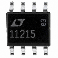
LT1121CS8-5#PBF Linear Technology, LT1121CS8-5#PBF Datasheet - Page 9

LT1121CS8-5#PBF
Manufacturer Part Number
LT1121CS8-5#PBF
Description
IC REG LDO 5V 150MA 8-SOIC
Manufacturer
Linear Technology
Specifications of LT1121CS8-5#PBF
Regulator Topology
Positive Fixed
Voltage - Output
5V
Voltage - Input
Up to 30V
Voltage - Dropout (typical)
0.42V @ 150mA
Number Of Regulators
1
Current - Output
150mA
Operating Temperature
0°C ~ 125°C
Mounting Type
Surface Mount
Package / Case
8-SOIC (3.9mm Width)
Primary Input Voltage
30V
Output Voltage Fixed
5V
Dropout Voltage Vdo
420mV
No. Of Pins
8
Output Current
150mA
Operating Temperature Range
0°C To +125°C
Msl
MSL 1 - Unlimited
Rohs Compliant
Yes
Lead Free Status / RoHS Status
Lead free / RoHS Compliant
Current - Limit (min)
-
Available stocks
Company
Part Number
Manufacturer
Quantity
Price
APPLICATIO S I FOR ATIO
Timing and Control
Conversion start and data read operations are controlled
by three digital inputs: CONVST, CS and RD. A falling edge
applied to the CONVST pin will start a conversion after the
ADC has been selected (i.e., CS is low). Once initiated, it
cannot be restarted until the conversion is complete.
Converter status is indicated by the BUSY output. BUSY is
low during a conversion.
We recommend using a narrow logic low or narrow logic
high CONVST pulse to start a conversion as shown in
Figures 5 and 6. A narrow low or high CONVST pulse
prevents the rising edge of the CONVST pulse from upset-
ting the critical bit decisions during the conversion time.
Figure 4 shows the change of the differential nonlinearity
error versus the low time of the CONVST pulse. As shown,
if CONVST returns high early in the conversion (e.g.,
CONVST low time <300ns), accuracy is unaffected. Simi-
larly, if CONVST returns high after the conversion is over
Figure 4. Change in DNL vs CONVST Low Time. Be Sure the
CONVST Pulse Returns High Early in the Conversion or After
the End of Conversion
4
3
2
1
0
0
CONVST
Figure 3. CS top CONVST Setup Timing
250
RD
CS
500
U
t
CONV
CONVST LOW TIME, t
t
750
1
t
2
U
1000
W
1250
5
(ns)
1608 F03
1500
t
U
ACQ
1750
1608 F04
2000
(e.g., CONVST low time >t
For best results, keep t
t
Figures 5 through 9 show several different modes of
operation. In modes 1a and 1b (Figures 5 and 6), CS and
RD are both tied low. The falling edge of CONVST starts the
conversion. The data outputs are always enabled and data
can be latched with the BUSY rising edge. Mode 1a shows
operation with a narrow logic low CONVST pulse. Mode 1b
shows a narrow logic high CONVST pulse.
In mode 2 (Figure 7) CS is tied low. The falling edge of
CONVST signal starts the conversion. Data outputs are in
three-state until read by the MPU with the RD signal. Mode
2 can be used for operation with a shared data bus.
In slow memory and ROM modes (Figures 8 and 9), CS is
tied low and CONVST and RD are tied together. The MPU
starts the conversion and reads the output with the com-
bined CONVST-RD signal. Conversions are started by the
MPU or DSP (no external sample clock is needed).
In slow memory mode, the processor applies a logic low
to RD (= CONVST), starting the conversion. BUSY goes
low, forcing the processor into a wait state. The previous
conversion result appears on the data outputs. When the
conversion is complete, the new conversion results
appear on the data outputs; BUSY goes high, releasing the
processor and the processor takes RD (= CONVST) back
high and reads the new conversion data.
In ROM mode, the processor takes RD (= CONVST) low,
starting a conversion and reading the previous conversion
result. After the conversion is complete, the processor can
read the new result and initiate another conversion.
DIFFERENTIAL ANALOG INPUTS
Driving the Analog Inputs
The differential analog inputs of the LTC1608 are easy to
drive. The inputs may be driven differentially or as a single-
ended input (i.e., the A
A
wanted signal that is common mode to both inputs will be
reduced by the common mode rejection of the sample-
and-hold circuit. The inputs draw only one small current
CONV
IN
–
.
inputs are sampled at the same instant. Any un-
IN
5
–
less than 500ns or greater than
input is grounded). The A
CONV
), accuracy is unaffected.
LTC1608
IN
+
9
and


