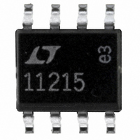
LT1121CS8-5#PBF Linear Technology, LT1121CS8-5#PBF Datasheet - Page 8

LT1121CS8-5#PBF
Manufacturer Part Number
LT1121CS8-5#PBF
Description
IC REG LDO 5V 150MA 8-SOIC
Manufacturer
Linear Technology
Specifications of LT1121CS8-5#PBF
Regulator Topology
Positive Fixed
Voltage - Output
5V
Voltage - Input
Up to 30V
Voltage - Dropout (typical)
0.42V @ 150mA
Number Of Regulators
1
Current - Output
150mA
Operating Temperature
0°C ~ 125°C
Mounting Type
Surface Mount
Package / Case
8-SOIC (3.9mm Width)
Primary Input Voltage
30V
Output Voltage Fixed
5V
Dropout Voltage Vdo
420mV
No. Of Pins
8
Output Current
150mA
Operating Temperature Range
0°C To +125°C
Msl
MSL 1 - Unlimited
Rohs Compliant
Yes
Lead Free Status / RoHS Status
Lead free / RoHS Compliant
Current - Limit (min)
-
Available stocks
Company
Part Number
Manufacturer
Quantity
Price
APPLICATIO S I FOR ATIO
LTC1608
compared with the binary-weighted charges supplied by
the differential capacitive DAC. Bit decisions are made by
the high speed comparator. At the end of a conversion, the
differential DAC output balances the A
charges. The SAR contents (a 16-bit data word) which
represent the difference of A
the 16-bit output latches.
DIGITAL INTERFACE
The A/D converter is designed to interface with micropro-
cessors as a memory mapped device. The CS and RD
control inputs are common to all peripheral memory
interfacing. A separate CONVST is used to initiate a con-
version.
Internal Clock
The A/D converter has an internal clock that runs the A/D
conversion. The internal clock is factory trimmed to achieve
a typical conversion time of 1.45 s and a maximum
conversion time of 1.8 s over the full temperature range.
No external adjustments are required. The guaranteed
maximum acquisition time is 400ns. In addition, a through-
put time (acquisition + conversion) of 2 s and a minimum
sampling rate of 500ksps are guaranteed.
8
A
A
IN
IN
+
–
SAMPLE
SAMPLE
+V
Figure 1. Simplified Block Diagram
DAC
HOLD
HOLD
–V
U
DAC
C
C
+C
–C
SMPL
SMPL
DAC
DAC
U
IN
SAR
+
and A
ZEROING SWITCHES
W
–
+
HOLD
HOLD
COMP
16
IN
IN
–
+
LATCHES
OUTPUT
are loaded into
and A
U
IN
•
•
•
–
input
1608 F01
D15
D0
3V Input/Output Compatible
The LTC1608 operates on 5V supplies, which makes the
device easy to interface to 5V digital systems. This device
can also talk to 3V digital systems: the digital input pins
(SHDN, CS, CONVST and RD) of the LTC1608 recognize
3V or 5V inputs. The LTC1608 has a dedicated output
supply pin (OV
digital output pins (D0 to D15, BUSY) and allows the part
to talk to either 3V or 5V digital systems. The output is
two’s complement binary.
Power Shutdown
The LTC1608 provides two power shutdown modes, Nap
and Sleep, to save power during inactive periods. The Nap
mode reduces the power by 95% and leaves only the
digital logic and reference powered up. The wake-up time
from Nap to active is 200ns. In Sleep mode, all bias
currents are shut down and only leakage current remains
(about 1 A). Wake-up time from Sleep mode is much
longer since the reference circuit must power up and
settle. Sleep mode wake-up time is dependent on the
value of the capacitor connected to the REFCOMP (Pin 4).
The wake-up time is 80ms with the recommended 22 F
capacitor.
Shutdown is controlled by Pin 33 (SHDN). The ADC is in
shutdown when SHDN is low. The shutdown mode is
selected with Pin 32 (CS). When SHDN is low, CS low
selects nap and CS high selects sleep.
Figure 2b. SHDN to CONVST Wake-Up Timing
Figure 2a. Nap Mode to Sleep Mode Timing
CONVST
SHDN
SHDN
DD
CS
) that controls the output swings of the
t
t
4
3
1608 F02a
1608 F02b


