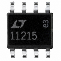
LT1121CS8-5#PBF Linear Technology, LT1121CS8-5#PBF Datasheet - Page 6

LT1121CS8-5#PBF
Manufacturer Part Number
LT1121CS8-5#PBF
Description
IC REG LDO 5V 150MA 8-SOIC
Manufacturer
Linear Technology
Specifications of LT1121CS8-5#PBF
Regulator Topology
Positive Fixed
Voltage - Output
5V
Voltage - Input
Up to 30V
Voltage - Dropout (typical)
0.42V @ 150mA
Number Of Regulators
1
Current - Output
150mA
Operating Temperature
0°C ~ 125°C
Mounting Type
Surface Mount
Package / Case
8-SOIC (3.9mm Width)
Primary Input Voltage
30V
Output Voltage Fixed
5V
Dropout Voltage Vdo
420mV
No. Of Pins
8
Output Current
150mA
Operating Temperature Range
0°C To +125°C
Msl
MSL 1 - Unlimited
Rohs Compliant
Yes
Lead Free Status / RoHS Status
Lead free / RoHS Compliant
Current - Limit (min)
-
Available stocks
Company
Part Number
Manufacturer
Quantity
Price
LTC1608
TYPICAL PERFOR A CE CHARACTERISTICS
PI FU CTIO S
A
difference voltage between A
tial range of 2.5V. A
A
A
to a DC voltage or driven differentially with A
V
2.2 F tantalum in parallel with 0.1 F ceramic.
REFCOMP (Pin 4): 4.375V (Nominal) Reference Compen-
sation Pin. Bypass to AGND with 22 F tantalum in parallel
with 0.1 F ceramic. This is not recommended for use as
an external reference due to part-to-part output voltage
variations and glitches that occur during the conversion.
AGND (Pins 5 to 8): Analog Grounds. Tie to analog ground
plane.
DV
with 10 F tantalum in parallel with 0.1 F ceramic.
DGND (Pin 10): Digital Ground for Internal Logic. Tie to
analog ground plane.
D15 to D0 (Pins 11 to 26): Three-State Data Outputs. D15
is the Most Significant Bit.
BUSY (Pin 27): The BUSY output shows the converter
status. It is low when a conversion is in progress. Data is
valid on the rising edge of BUSY.
6
IN
IN
IN
REF
–100
–120
–140
–20
–40
–60
–80
DD
U
+
–
–
0
(Pin 1): Positive Analog Input. The ADC converts the
(Pin 2): Negative Analog Input. Can be grounded, tied
0
(Pin 3): 2.5V Reference Output. Bypass to AGND with
is grounded.
Intermodulation Distortion
(Pin 9): 5V Digital Power Supply. Bypass to DGND
U
50
FREQUENCY (kHz)
100
U
IN
150
f
f
f
SAMPLE
IN1
IN2
+
has a 2.5V input range when
= 96.56kHz
= 99.98kHz
W
200
IN
= 500kHz
+
1608 G07
and A
U
250
IN
–
with a differen-
–100
–120
–140
–20
–40
–60
–80
0
IN
1k
Power Supply Feedthrough
vs Ripple Frequency
+
f
V
SAMPLE
.
RIPPLE
= 10mV
= 500kHz
INPUT FREQUENCY (Hz)
A
10k
VDD
OGND (Pin 28): Digital Ground for Output Drivers.
OV
Bypass to OGND with 10 F tantalum in parallel with 0.1 F
ceramic.
RD (Pin 30): Read Input. A logic low enables the output
drivers when CS is low.
CONVST (Pin 31): Conversion Start Signal. This active
low signal starts a conversion on its falling edge when CS
is low.
CS (Pin 32): The Chip Select Input. Must be low for the ADC
to recognize CONVST and RD inputs.
SHDN (Pin 33): Power Shutdown. Drive this pin low with
CS low for nap mode. Drive this pin low with CS high for
sleep mode.
V
10 F tantalum in parallel with 0.1 F ceramic.
AV
with 10 F tantalum in parallel with 0.1 F ceramic.
AV
with 10 F tantalum in parallel with 0.1 F ceramic and
connect this pin to Pin 35 with a 10 resistor.
SS
DD
DD
DD
(Pin 34): – 5V Negative Supply. Bypass to AGND with
100k
V
SS
(Pin 35): 5V Analog Power Supply. Bypass to AGND
(Pin 36): 5V Analog Power Supply. Bypass to AGND
(Pin 29): Digital Power Supply for Output Drivers.
1608 G08
1M
80
70
60
50
40
30
20
10
0
1k
Input Common Mode Rejection
vs Input Frequency
INPUT FREQUENCY (Hz)
10k
100k
1608 G14a
1M


