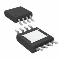
LT3085MPMS8E#TRPBF Linear Technology, LT3085MPMS8E#TRPBF Datasheet - Page 15

LT3085MPMS8E#TRPBF
Manufacturer Part Number
LT3085MPMS8E#TRPBF
Description
IC LDO REG ADJ 500MA 8-MSOP
Manufacturer
Linear Technology
Datasheet
1.LT3085EDCBTRMPBF.pdf
(28 pages)
Specifications of LT3085MPMS8E#TRPBF
Regulator Topology
Positive Adjustable
Voltage - Output
Adjustable
Voltage - Input
1.2 ~ 36 V
Voltage - Dropout (typical)
1.35V @ 500mA
Number Of Regulators
1
Current - Output
500mA
Current - Limit (min)
500mA
Operating Temperature
-55°C ~ 125°C
Mounting Type
Surface Mount
Package / Case
8-MSOP Exposed Pad, 8-HMSOP, 8-eMSOP
Lead Free Status / RoHS Status
Lead free / RoHS Compliant
Available stocks
Company
Part Number
Manufacturer
Quantity
Price
APPLICATIONS INFORMATION
If the LT3085 is confi gured as a three-terminal (single supply)
regulator with IN and V
diode of the IN pin will protect the V
Like any other regulator, exceeding the maximum input-
to-output differential causes internal transistors to break
down and then none of the internal protection circuitry
is functional.
Thermal Considerations
The LT3085 has internal power and thermal limiting cir-
cuitry designed to protect it under overload conditions.
For continuous normal load conditions, maximum junc-
tion temperature must not be exceeded. It is important
to give consideration to all sources of thermal resistance
from junction to ambient. This includes junction-to-case,
case-to-heat sink interface, heat sink resistance or circuit
board-to-ambient as the application dictates. Additional
heat sources nearby must also be considered.
For surface mount devices, heat sinking is accomplished
by using the heat spreading capabilities of the PC board
and its copper traces. Surface mount heat sinks and
plated through-holes can also be used to spread the heat
generated by power devices. Boards specifi ed in thermal
resistance tables have no vias on plated through-holes
from topside to backside.
Junction-to-case thermal resistance is specifi ed from
the IC junction to the bottom of the case directly below
the die. This is the lowest resistance path for heat fl ow.
Proper mounting is required to ensure the best possible
thermal fl ow from this area of the package to the heat
sinking material. Note that the Exposed Pad is electrically
connected to the output.
The following tables list thermal resistance for several
different copper areas given a fi xed board size. All mea-
surements were taken in still air on two-sided 1/16” FR-4
board with one ounce copper.
PCB layers, copper weight, board layout and thermal vias
affect the resultant thermal resistance. Although Tables
2 and 3 provide thermal resistance numbers for 2-layer
board with 1 ounce copper, modern multi-layer PCBs
CONTROL
shorted together, the internal
CONTROL
pin.
provide better performance than found in these tables.
For example, a 4-layer, 1 ounce copper PCB board with
5 thermal vias from the DFN or MSOP exposed backside
pad to inner layers (connected to V
thermal resistance. Demo circuit 1401A’s board layout
achieves this 40 °C/W performance. This is approximately
a 45% improvement over the numbers shown in Tables
2 and 3.
Table 2. MSE Package, 8-Lead MSOP
*Device is mounted on topside
Table 3. DCB Package, 6-Lead DFN
Calculating Junction Temperature
Example: Given an output voltage of 0.9V, a V
voltage of 3.3V ±10%, an IN voltage of 1.5V ±5%, output
current range from 1mA to 0.5A and a maximum ambi-
ent temperature of 50°C, what will the maximum junction
temperature be for the DFN package on a 2500mm
with topside copper area of 500mm
The power in the drive circuit equals:
where I
of output current. A curve of I
in the Typical Performance Characteristics curves.
*Device is mounted on topside
For future information on the thermal resistance and using thermal
information, refer to JEDEC standard JESD51, notably JESD51-12.
TOPSIDE*
TOPSIDE*
2500mm
1000mm
2500mm
1000mm
225mm
100mm
225mm
100mm
P
DRIVE
COPPER AREA
COPPER AREA
CONTROL
2
2
2
2
2
2
2
2
= (V
BACKSIDE
BACKSIDE
2500mm
2500mm
2500mm
2500mm
2500mm
2500mm
2500mm
2500mm
CONTROL
is equal to I
2
2
2
2
2
2
2
2
BOARD AREA
BOARD AREA
– V
2500mm
2500mm
2500mm
2500mm
2500mm
2500mm
2500mm
2500mm
OUT
OUT
CONTROL
)(I
2
2
2
2
2
2
2
2
/60. I
CONTROL
OUT
(JUNCTION-TO-AMBIENT)
(JUNCTION-TO-AMBIENT)
2
CONTROL
THERMAL RESISTANCE
THERMAL RESISTANCE
vs I
?
) achieves 40 °C/W
OUT
)
55°C/W
57°C/W
60°C/W
65°C/W
68°C/W
70°C/W
73°C/W
78°C/W
LT3085
can be found
is a function
CONTROL
15
2
board
3085fb


