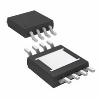
LT3085MPMS8E#TRPBF Linear Technology, LT3085MPMS8E#TRPBF Datasheet - Page 7

LT3085MPMS8E#TRPBF
Manufacturer Part Number
LT3085MPMS8E#TRPBF
Description
IC LDO REG ADJ 500MA 8-MSOP
Manufacturer
Linear Technology
Datasheet
1.LT3085EDCBTRMPBF.pdf
(28 pages)
Specifications of LT3085MPMS8E#TRPBF
Regulator Topology
Positive Adjustable
Voltage - Output
Adjustable
Voltage - Input
1.2 ~ 36 V
Voltage - Dropout (typical)
1.35V @ 500mA
Number Of Regulators
1
Current - Output
500mA
Current - Limit (min)
500mA
Operating Temperature
-55°C ~ 125°C
Mounting Type
Surface Mount
Package / Case
8-MSOP Exposed Pad, 8-HMSOP, 8-eMSOP
Lead Free Status / RoHS Status
Lead free / RoHS Compliant
Available stocks
Company
Part Number
Manufacturer
Quantity
Price
PIN FUNCTIONS
TYPICAL PERFORMANCE CHARACTERISTICS
V
control circuitry of the device. The current fl ow into this
pin is about 1.7% of the output current. For the device to
regulate, this voltage must be more than 1.2V to 1.35V
greater than the output voltage (see V
Voltage in the Electrical Characteristics table and graphs
in the Typical Performance Characteristics). The LT3085
requires a bypass capacitor at V
inches away from the main input fi lter capacitor. The output
impedance of a battery rises with frequency, so include
a bypass capacitor in battery-powered circuits. A bypass
capacitor in the range of 1μF to 10μF suffi ces.
IN (Pins 5, 6/Pins 7, 8): This is the collector to the power
device of the LT3085. The output load current is supplied
through this pin. For the device to regulate, the voltage at
this pin must be more than 0.1V to 0.5V greater than the
output voltage (see V
Characteristics table and graphs in the Typical Perfor-
mance Characteristics). The LT3085 requires a bypass
capacitor at IN if more than six inches away from the main
input fi lter capacitor. The output impedance of a battery
CONTROL
(Pin 4/Pin 5): This pin is the supply pin for the
21
18
15
12
–3
–6
–9
9
6
3
0
10
Error Amplifi er Gain and Phase
IN
Dropout Voltage in the Electrical
100
(DCB/MS8E)
FREQUENCY (Hz)
I
LOAD
I
LOAD
1k
CONTROL
= 500mA
= 100mA
10k
I
LOAD
I
LOAD
CONTROL
= 100mA
if more than six
= 500mA
100k
3085 G28
Dropout
1M
216
144
72
0
–72
–144
–216
–288
–360
–432
–504
rises with frequency, so include a bypass capacitor in
battery-powered circuits. A bypass capacitor in the range
of 1μF to 10μF suffi ces.
NC (NA/Pin 6): No Connection. The No Connect pin has
no connection to internal circuitry and may be tied to V
V
OUT (Pins 1, 2/Pins 1, 2, 3): This is the power output
of the device. There must be a minimum load current of
1mA or the output may not regulate. A minimum 2.2μF
output capacitor is required for stability.
SET (Pin 3/Pin 4): This pin is the non-inverting input to the
error amplifi er and the regulation set point for the device.
A fi xed current of 10μA fl ows out of this pin through a
single external resistor, which programs the output voltage
of the device. Output voltage range is zero to the absolute
maximum rated output voltage. Transient performance can
be improved and output noise can be decreased by adding
a small capacitor from the SET pin to ground.
Exposed Pad (Pin 7/Pin 9): OUT. Tie directly to Pins 1, 2/
Pins 2, 3 directly at the PCB.
CONTROL
150
135
120
105
90
75
60
45
30
15
0
10
, V
Ripple Rejection - SET Pin Current
R
V
RIPPLE = 50mV
OUT
IN
SET
= V
100
= 100k
, GND, or fl oated.
CONTROL
C
SET
C
FREQUENCY (Hz)
SET
= 0
1k
P–P
= V
= 0.1μF
OUT (NOMINAL)
10k
100k
+2V
3085 G29
1M
LT3085
3085fb
7
IN
,


