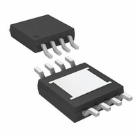
LT3085MPMS8E#TRPBF Linear Technology, LT3085MPMS8E#TRPBF Datasheet - Page 8

LT3085MPMS8E#TRPBF
Manufacturer Part Number
LT3085MPMS8E#TRPBF
Description
IC LDO REG ADJ 500MA 8-MSOP
Manufacturer
Linear Technology
Datasheet
1.LT3085EDCBTRMPBF.pdf
(28 pages)
Specifications of LT3085MPMS8E#TRPBF
Regulator Topology
Positive Adjustable
Voltage - Output
Adjustable
Voltage - Input
1.2 ~ 36 V
Voltage - Dropout (typical)
1.35V @ 500mA
Number Of Regulators
1
Current - Output
500mA
Current - Limit (min)
500mA
Operating Temperature
-55°C ~ 125°C
Mounting Type
Surface Mount
Package / Case
8-MSOP Exposed Pad, 8-HMSOP, 8-eMSOP
Lead Free Status / RoHS Status
Lead free / RoHS Compliant
Available stocks
Company
Part Number
Manufacturer
Quantity
Price
LT3085
BLOCK DIAGRAM
APPLICATIONS INFORMATION
The LT3085 regulator is easy to use and has all the pro-
tection features expected in high performance regulators.
Included are short-circuit protection and safe operating
area protection, as well as thermal shutdown.
The LT3085 is especially well suited to applications needing
multiple rails. The new architecture adjusts down to zero
with a single resistor, handling modern low voltage digital
IC’s as well as allowing easy parallel operation and thermal
management without heat sinks. Adjusting to “zero” output
allows shutting off the powered circuitry and when the
input is pre-regulated – such as a 5V or 3.3V input supply
– external resistors can help spread the heat.
A precision “0” TC 10μA internal current source is connected
to the non-inverting input of a power operational amplifi er.
The power operational amplifi er provides a low impedance
buffered output to the voltage on the non-inverting input.
A single resistor from the non-inverting input to ground
sets the output voltage and if this resistor is set to zero,
zero output results. As can be seen, any output voltage
can be obtained from zero up to the maximum defi ned by
the input power supply.
8
V
CONTROL
IN
SET
10μA
–
+
What is not so obvious from this architecture are the ben-
efi ts of using a true internal current source as the reference
as opposed to a bootstrapped reference in older regulators.
A true current source allows the regulator to have gain
and frequency response independent of the impedance on
the positive input. Older adjustable regulators, such as the
LT1086, have a change in loop gain with output voltage
as well as bandwidth changes when the adjustment pin
is bypassed to ground. For the LT3085, the loop gain is
unchanged by changing the output voltage or bypassing.
Output regulation is not fi xed at a percentage of the output
voltage but is a fi xed fraction of millivolts. Use of a true
current source allows all the gain in the buffer amplifi er
to provide regulation and none of that gain is needed to
amplify up the reference to a higher output voltage.
The LT3085 has the collector of the output transistor
connected to a separate pin from the control input. Since the
dropout on the collector (IN pin) is only 275mV, two supplies
can be used to power the LT3085 to reduce dissipation: a
higher voltage supply for the control circuitry and a lower
voltage supply for the collector. This increases effi ciency and
reduces dissipation. To further spread the heat, a resistor
can be inserted in series with the collector to move some
of the heat out of the IC and spread it on the PC board.
OUT
3085 BD
3085fb


