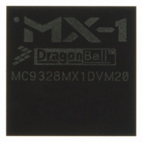
MC9328MX1DVM20 Freescale Semiconductor, MC9328MX1DVM20 Datasheet - Page 22

MC9328MX1DVM20
Manufacturer Part Number
MC9328MX1DVM20
Description
IC MCU I.MX 200MHZ 256-MAPBGA
Manufacturer
Freescale Semiconductor
Series
i.MX1r
Datasheet
1.MC9328MX1DVH20.pdf
(100 pages)
Specifications of MC9328MX1DVM20
Core Processor
ARM9
Core Size
32-Bit
Speed
200MHz
Connectivity
EBI/EMI, I²C, MMC, SmartCard, SPI, SSI, UART/USART, USB
Peripherals
DMA, I²S, LCD, POR, PWM, WDT
Number Of I /o
110
Program Memory Type
ROMless
Voltage - Supply (vcc/vdd)
1.7 V ~ 3.3 V
Oscillator Type
External
Operating Temperature
-30°C ~ 70°C
Package / Case
256-MAPBGA
Lead Free Status / RoHS Status
Lead free / RoHS Compliant
Eeprom Size
-
Ram Size
-
Program Memory Size
-
Data Converters
-
Available stocks
Company
Part Number
Manufacturer
Quantity
Price
Company:
Part Number:
MC9328MX1DVM20
Manufacturer:
Freescale Semiconductor
Quantity:
10 000
Company:
Part Number:
MC9328MX1DVM20R2
Manufacturer:
Freescale Semiconductor
Quantity:
10 000
Electrical Characteristics
3
This section contains the electrical specifications and timing diagrams for the i.MX1 processor.
3.1
Table 4
device may occur. Functional operation should be restricted to the limits listed in Recommended Operating
Range
3.2
Table 5
processor has multiple pairs of VDD and VSS power supply and return pins. QVDD and QVSS pins are
used for internal logic. All other VDD and VSS pins are for the I/O pads voltage supply, and each pair of
VDD and VSS provides power to the enclosed I/O pads. This design allows different peripheral supply
voltage levels in a system.
Because AVDD pins are supply voltages to the analog pads, it is recommended to isolate and noise-filter
the AVDD pins from other VDD pins.
BTRFVDD is the supply voltage for the Bluetooth interface signals. It is quite sensitive to the data
transmit/receive accuracy. Please refer to Bluetooth RF spec for special handling. If Bluetooth is not used
22
1
2
A typical application with 30 pads simultaneously switching assumes the GPIO toggling and instruction fetches from the ARM
core-that is, 7x GPIO, 15x Data bus, and 8x Address bus.
A worst-case application with 70 pads simultaneously switching assumes the GPIO toggling and instruction fetches from the
ARM core-that is, 32x GPIO, 30x Data bus, 8x Address bus. These calculations are based on the core running its heaviest OS
application at MHz, and where the whole image is running out of SDRAM. QVDD at V, NVDD and AVDD at 3.3V, therefore,
180mA is the worst measurement recorded in the factory environment, max 5mA is consumed for OSC pads, with each toggle
GPIO consuming 4mA.
VESD_HBM
VESD_MM
BTRFV
ILatchup
Symbol
QV
QV
NV
AV
Pmax
Table 5 on page 23
Test
Electrical Characteristics
provides the recommended operating ranges for the supply voltages and temperatures. The i.MX1
provides information on maximum ratings which are those values beyond which damage to the
DD
DD
DD
DD
Maximum Ratings
Recommended Operating Range
DD
DC I/O Supply Voltage
DC Internal (core = 150 MHz) Supply Voltage
DC Internal (core = 200 MHz) Supply Voltage
DC Analog Supply Voltage
DC Bluetooth Supply Voltage
ESD immunity with HBM (human body model)
ESD immunity with MM (machine model)
Latch-up immunity
Storage temperature
Power Consumption
or the DC Characteristics table.
MC9328MX1 Technical Data, Rev. 7
Rating
Table 4. Maximum Ratings
Minimum
800
-0.3
-0.3
-0.3
-0.3
-0.3
-55
–
–
–
1
Freescale Semiconductor
Maximum
1300
2000
100
200
150
3.3
1.9
2.0
3.3
3.3
2
Unit
mW
mA
°C
V
V
V
V
V
V
V
®


