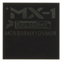
MC9328MX1DVM20 Freescale Semiconductor, MC9328MX1DVM20 Datasheet - Page 69

MC9328MX1DVM20
Manufacturer Part Number
MC9328MX1DVM20
Description
IC MCU I.MX 200MHZ 256-MAPBGA
Manufacturer
Freescale Semiconductor
Series
i.MX1r
Datasheet
1.MC9328MX1DVH20.pdf
(100 pages)
Specifications of MC9328MX1DVM20
Core Processor
ARM9
Core Size
32-Bit
Speed
200MHz
Connectivity
EBI/EMI, I²C, MMC, SmartCard, SPI, SSI, UART/USART, USB
Peripherals
DMA, I²S, LCD, POR, PWM, WDT
Number Of I /o
110
Program Memory Type
ROMless
Voltage - Supply (vcc/vdd)
1.7 V ~ 3.3 V
Oscillator Type
External
Operating Temperature
-30°C ~ 70°C
Package / Case
256-MAPBGA
Lead Free Status / RoHS Status
Lead free / RoHS Compliant
Eeprom Size
-
Ram Size
-
Program Memory Size
-
Data Converters
-
Available stocks
Company
Part Number
Manufacturer
Quantity
Price
Company:
Part Number:
MC9328MX1DVM20
Manufacturer:
Freescale Semiconductor
Quantity:
10 000
Company:
Part Number:
MC9328MX1DVM20R2
Manufacturer:
Freescale Semiconductor
Quantity:
10 000
4.10.1
The card identification and card operation conditions timing are processed in open-drain mode. The card
response to the host command starts after exactly N
SET_RCA is also processed in the open-drain mode. The minimum delay between the host command and
card response is NCR clock cycles as illustrated in
Figure 52
Freescale Semiconductor
1
2
3
Ref
No.
C
C
C
3a
3b
4a
4b
5a
5b
6a
6b
1
2
7
L
L
L
≤
≤
≤
100 pF / 250 pF (10/30 cards)
25 pF (1 card)
are defined in
250 pF (21 cards)
CLK frequency at Data transfer Mode
(PP)
CLK frequency at Identification Mode
Clock high time
Clock low time
Clock fall time
Clock rise time
Input hold time
Input setup time
Output hold time
Output setup time
Output delay time
Symbol
Command Response Timing on MMC/SD Bus
CRC
D
1
Z
*
—10/30 cards
Table 29. State Signal Parameters for
Cyclic redundancy check bits (7 bits)
1
1
1
3
—10/30 cards
1
Parameter
—10/30 cards
—10/30 cards
—10/30 cards
3
—10/30 cards
3
Table
—10/30 cards
—10/30 cards
3
3
—10/30 cards
Card Active
High impedance state
Table 28. SDHC Bus Timing Parameter Table
29.
Definition
Repetition
Data bits
MC9328MX1 Technical Data, Rev. 7
2
Minimum
10.3/10.3
10.3/10.3
5.7/5.7
5.7/5.7
15/75
6/33
Figure
0
0
–
–
0
ID
1.8 ± 0.1 V
clock cycles. For the card address assignment,
Symbol
S
P
E
Figure 48
T
48. The symbols for
Maximum
(5.00)
(6.67)
10/50
14/67
25/5
400
16
–
–
–
–
–
–
Transmitter bit (Host = 1, Card = 0)
Functional Description and Application Information
3
3
through
Host Active
One-cycle pull-up (1)
Minimum
10/50
10/50
Start bit (0)
Definition
End bit (1)
9/9
9/9
5/5
5/5
0
0
–
–
0
Figure 52
3.0 ± 0.3 V
Figure 48
Maximum
10/50
10/50
25/5
400
14
–
–
–
–
–
–
through
MHz
Unit
kHz
ns
ns
ns
ns
ns
ns
ns
ns
ns
69


