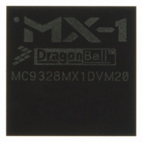
MC9328MX1DVM20 Freescale Semiconductor, MC9328MX1DVM20 Datasheet - Page 61

MC9328MX1DVM20
Manufacturer Part Number
MC9328MX1DVM20
Description
IC MCU I.MX 200MHZ 256-MAPBGA
Manufacturer
Freescale Semiconductor
Series
i.MX1r
Datasheet
1.MC9328MX1DVH20.pdf
(100 pages)
Specifications of MC9328MX1DVM20
Core Processor
ARM9
Core Size
32-Bit
Speed
200MHz
Connectivity
EBI/EMI, I²C, MMC, SmartCard, SPI, SSI, UART/USART, USB
Peripherals
DMA, I²S, LCD, POR, PWM, WDT
Number Of I /o
110
Program Memory Type
ROMless
Voltage - Supply (vcc/vdd)
1.7 V ~ 3.3 V
Oscillator Type
External
Operating Temperature
-30°C ~ 70°C
Package / Case
256-MAPBGA
Lead Free Status / RoHS Status
Lead free / RoHS Compliant
Eeprom Size
-
Ram Size
-
Program Memory Size
-
Data Converters
-
Available stocks
Company
Part Number
Manufacturer
Quantity
Price
Company:
Part Number:
MC9328MX1DVM20
Manufacturer:
Freescale Semiconductor
Quantity:
10 000
Company:
Part Number:
MC9328MX1DVM20R2
Manufacturer:
Freescale Semiconductor
Quantity:
10 000
4.6.2
The ideal mapping of input voltage to output digital sample is defined as follows:
In general, the mapping function is:
Where V is input, S is output, G is the slope, and C is the y-intercept.
Nominal Gain G
Nominal Offset C
4.6.3
The ideal mapping of input voltage to output digital sample is defined as:
In general, the mapping function is:
Where V is input, S is output, G is the slope, and C is the y-intercept.
Nominal Gain G
Nominal Offset C
Freescale Semiconductor
S = G * V + C
S = G * V + C
Gain Calculations
Offset Calculations
0
0
0
0
-2400
= 65535 / 4800 = 13.65mV
= 65535 / 4800 = 13.65mV
-2400
= 65535 / 2 = 32767
= 65535 / 2 = 32767
MC9328MX1 Technical Data, Rev. 7
Figure 35. Offset Calculations
Figure 34. Gain Calculations
65535
Smax
65535
Smax
Sample
-1
-1
Sample
C0
C0
Functional Description and Application Information
1800
1800
2400
2400
G0
G0
Vi
Vi
61


