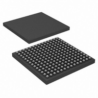
ISL5239KIZ Intersil, ISL5239KIZ Datasheet - Page 14

ISL5239KIZ
Manufacturer Part Number
ISL5239KIZ
Description
IC LINEARIZER PRE-DISTORT 196BGA
Manufacturer
Intersil
Datasheet
1.ISL5239EVAL1.pdf
(31 pages)
Specifications of ISL5239KIZ
Function
Pre-Distortion Linearizer
Rf Type
CDMA2000, UMTS
Secondary Attributes
Sample Rates to 125MSPS
Package / Case
196-BGA
Lead Free Status / RoHS Status
Lead free / RoHS Compliant
Available stocks
Company
Part Number
Manufacturer
Quantity
Price
Part Number:
ISL5239KIZ
Manufacturer:
INTERSIL
Quantity:
20 000
Read Access to the Capture Memory
Correction Filter Read/Write Procedure
Write Access to the Correction Filter Coefficients
Read Access to the Correction Filter Coefficients
Latency
To be provided later.
Reset
There are three types of chip resets.
RESET pin
A hard reset can occur by asserting the input pin RESET
which resets all chip registers to their default condition, and
resets the uP interface.
1. Perform a direct write to control word 0x04 by setting up
2. Perform a direct read of 0x0c by dropping the RD line low
3. Perform a direct read of control word 0x0d by dropping the
1. Perform a direct write to control word 0x28 by setting up
2. Perform a direct write to control word 0x29 by setting up
3. Perform a direct write to control word 0x2a by setting up
4. Repeat step 3 until all 13 coefficients for I and for Q have
1. Perform a direct write to control word 0x028 by setting up
2. Perform a direct write to control word 0x029 by setting up
3. Perform a direct read of 0x2a by dropping the RD line low
the address on A<5:0>, data on P<15:0>, and generating
a rising edge on WR. 0x04 selects the auto increment
mode and the input or feedback memories.
to transfer data from the slave register selected by
A<5:0> onto the data bus P<15:0>.
RD line low to transfer data from the slave register
selected by A<5:0> onto the data bus P<15:0>. Reading
from this control word performs the auto increment, if
enabled.
the address on A<5:0>, data on P<15:0>, and generating
a rising edge on WR. 0x28 selects the auto increment
mode.
the address on A<5:0>, data on P<15:0>, and generating
a rising edge on WR. 0x29 selects the coefficient address
for I or Q.
the address on A<5:0>, data on P<15:0>, and generating
a rising edge on WR.
been loaded as the master registers are transferred to the
slaves when the last Q coefficient is written.
the address on A<5:0>, data on P<15:0>, and generating
a rising edge on WR. 0x28 selects the auto increment
mode.
the address on A<5:0>, data on P<15:0>, and generating
a rising edge on WR.
to transfer data from the slave register selected by
A<5:0> onto the data bus P<15:0>.
14
ISL5239
Software Hard Reset
The µP can issue a reset command through the global
control register 0x00, bit 4. This reset is identical to asserting
the RESET pin, except the control fields 0x00 and 0x01 are
not affected, and the uP interface is not reset.
Software Soft Reset
The uP can issue a reset command through the global
control register 0x00, bit 0, which is identical to a Software
hard reset, but none of the control registers are reset. A soft
reset leaves the device in an idle state.
JTAG Test
The IEEE 1149.1 Joint Test Action Group boundary scan
standard operational codes shown in Table 9 are supported.
A separate application note is available with implementation
details and the BSDL file is available.
Power-up Sequencing
The ISL5239 core and I/O blocks are isolated by structures
which may become forward biased if the supply voltages are
not at specified levels. During the power-up and power-down
operations, differences in the starting point and ramp rates of
the two supplies may cause current to flow in the isolation
structures which, when prolonged and excessive, can
reduce the usable life of the device. In general, the most
preferred case would be to power-up or down the core and
I/O structures simultaneously. However, it is also safe to
power-up the core prior to the I/O block if simultaneous
application of the supplies is not possible. In this case, the
I/O voltage should be applied within 10 ms to 100 ms
nominally to preserve component reliability. Bringing the
core and I/O supplies to their respective regulation levels in
a maximum time frame of a 100 ms, moderates the stresses
placed on both, the power supply and the ISL5239. When
powering down, simultaneous removal is preferred, but It is
also safe to remove the I/O supply prior to the core supply. If
the core power is removed first, the I/O supply should also
be removed within 10-100mS.
Application Notes and Evaluation Boards
The ISL5239 operation can be demonstrated via the
ISL5239EVAL1 board. All required hardware and Windows
GUI software are supplied with both a user’s manual and
accompanying applications notes.
TABLE 1. JTAG OP CODES SUPPORTED
SAMPLE/PRELOAD
INSTRUCTION
BYPASS
EXTEST
IDCODE
INTEST
OP CODE
0000
0001
0010
0011
1111


