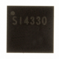
SI4330-B1-FM Silicon Laboratories Inc, SI4330-B1-FM Datasheet - Page 42

SI4330-B1-FM
Manufacturer Part Number
SI4330-B1-FM
Description
IC RCVR ISM 960MHZ 3.6V 20-QFN
Manufacturer
Silicon Laboratories Inc
Type
ISM Receiverr
Specifications of SI4330-B1-FM
Package / Case
20-QFN
Frequency
960MHz
Sensitivity
-118dBm
Data Rate - Maximum
128kbps
Modulation Or Protocol
FSK, GFSK, OOK
Current - Receiving
18.5mA
Data Interface
PCB, Surface Mount
Antenna Connector
PCB, Surface Mount
Voltage - Supply
1.8 V ~ 3.6 V
Operating Temperature
-40°C ~ 85°C
Operating Frequency
240 MHz to 960 MHz
Operating Supply Voltage
3 V
Maximum Operating Temperature
+ 85 C
Minimum Operating Temperature
- 40 C
Mounting Style
SMD/SMT
Supply Current
18.5 mA
Package
20QFN EP
Maximum Data Rate
256 Kbps
Transmission Media Type
Wireless
Power Supply Type
Analog
Typical Operating Supply Voltage
3 V
Minimum Operating Supply Voltage
1.8 V
Maximum Operating Supply Voltage
3.6 V
Lead Free Status / RoHS Status
Lead free / RoHS Compliant
Features
-
Applications
-
Memory Size
-
Lead Free Status / Rohs Status
Lead free / RoHS Compliant
Other names
336-1629-5
SI4330-V2-FM
SI4330-V2-FM
Available stocks
Company
Part Number
Manufacturer
Quantity
Price
Part Number:
SI4330-B1-FM
Manufacturer:
SILICON LABS/芯科
Quantity:
20 000
Company:
Part Number:
SI4330-B1-FM-02T
Manufacturer:
SILICON
Quantity:
112
Company:
Part Number:
SI4330-B1-FMR
Manufacturer:
HIROSE
Quantity:
3 200
Part Number:
SI4330-B1-FMR
Manufacturer:
SILICON LABS/芯科
Quantity:
20 000
Si4330-B1
8.3. General Purpose ADC
An 8-bit SAR ADC is integrated for general purpose use, as well as for digitizing the on-chip temperature sensor
reading. Registers 0Fh "ADC Configuration", 10h "Sensor Offset" and 4Fh "Amplifier Offset" can be used to
configure the ADC operation.
Every time an ADC conversion is desired, bit 7 "adcstart/adcbusy" in “Register 1Fh. Clock Recovery Gearshift
Override” must be set to 1. This is a self clearing bit that will be reset to 0 at the end of the conversion cycle of the
ADC. The conversion time for the ADC is 350 µs. After this time or when the "adcstart/adcbusy" bit is cleared, then
the ADC value may be read out of register 11h "ADC Value".
The architecture of the ADC is shown in Figure 19. The signal and reference inputs of the ADC are selected by
adcsel[2:0] and adcref[1:0] in “Register 0Fh. ADC Configuration,” respectively. The default setting is to read out the
temperature sensor using the bandgap voltage (VBG) as reference. With the VBG reference the input range of the
ADC is from 0–1.02 V with an LSB resolution of 4 mV (1.02/255). Changing the ADC reference will change the LSB
resolution accordingly.
A differential multiplexer and amplifier are provided for interfacing external bridge sensors. The gain of the amplifier
is selectable by adcgain[1:0] in Register 0Fh. The majority of sensor bridges have supply voltage (VDD) dependent
gain and offset. The reference voltage of the ADC can be changed to either V
dependent offset voltage can be added using soffs[3:0] in register 10h.
See “AN448: General Purpose ADC Configuration” for more details on the usage of the general purpose ADC.
42
Add
0F
10
11
R/W
R/W
R/W
R
Function/Description
ADC Configuration
Sensor Offset
ADC Value
GPIO0
GPIO1
GPIO2
Temperature Sensor
V
V
V
DD
DD
BG
(1.2V)
/ 3
/ 2
Figure 19. General Purpose ADC Architecture
adcsel [2:0]
Diff. MUX
adcstart/adcbusy
adc[7]
D7
aoffs [4:0]
adcgain [1:0]
Diff. Amp.
adcsel[2] adcsel[1]
adc[6]
soffs [3:0]
D6
Rev 1.0
adc[5]
D5
adcsel [2:0]
Input MUX
adcref [1:0]
Ref MUX
adcsel[0]
adc[4]
D4
V
V
adcref[1]
soffs[3]
in
ref
adc[3]
D3
0 -1020mV / 0-255
8-bit ADC
DD
/2 or V
adcref[0]
soffs[2]
adc[2]
D2
DD
adc [7:0]
adcgain[1] adcgain[0]
/3. A programmable V
soffs[1]
adc[1]
D1
soffs[0]
adc[0]
D0
POR Def.
00h
00h
—
DD


