CYWUSB6934-28SEC Cypress Semiconductor Corp, CYWUSB6934-28SEC Datasheet - Page 21
CYWUSB6934-28SEC
Manufacturer Part Number
CYWUSB6934-28SEC
Description
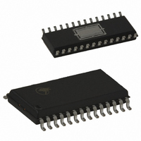
IC WIRELESS USB 2.4GHZ 28-SOIC
Manufacturer
Cypress Semiconductor Corp
Specifications of CYWUSB6934-28SEC
Frequency
2.4GHz
Data Rate - Maximum
62.5kbps
Modulation Or Protocol
DSSS, GFSK
Applications
HID, PC, Peripheral Gaming Devices
Power - Output
0dBm
Sensitivity
-90dBm
Voltage - Supply
2.7 V ~ 3.6 V
Data Interface
PCB, Surface Mount
Antenna Connector
PCB, Surface Mount
Operating Temperature
0°C ~ 70°C
Package / Case
28-SOIC
Operating Temperature (min)
0C
Operating Temperature (max)
70C
Operating Temperature Classification
Commercial
Operating Supply Voltage (min)
2.7V
Operating Supply Voltage (typ)
3V
Operating Supply Voltage (max)
3.6V
Lead Free Status / RoHS Status
Contains lead / RoHS non-compliant
Memory Size
-
Current - Transmitting
-
Current - Receiving
-
Lead Free Status / Rohs Status
Not Compliant
Other names
428-1580-5
Available stocks
Company
Part Number
Manufacturer
Quantity
Price
Company:

Part Number:
CYWUSB6934-28SEC
Manufacturer:
CY
Quantity:
22 751


Table 30. Carrier Detect
Table 31. Clock Manual
Table 32. Clock Enable
Table 33. Synthesizer Lock Count
Table 34. Manufacturing ID
Document 38-16007 Rev. *J
7
6:0
7:0
7:0
7:0
31:30
29:0
31 30 29 28 27 26 25 24 23 22 21 20 19 18 17 16 15 14 13 12 11 10
Carrier Detect
Bit
Bit Name
Bit
Bit
Bit
Override
Carrier Detect Override When set, this bit overrides carrier detect. The user must set Reg 0x20, bit 6=1 to enable writes to
Reserved
Count Determines the length of delay in 2µs increments for the synthesizer to lock when auto synthesizer is enabled via
Manual Clock
Enables
Manual Clock Overrides This register must be written with 0x41 after reset for correct operation
7
7
7
7
Address[31:3
0]
Address[29:0] These bits are the Manufacturing ID (MID) for each IC. The contents of these bits cannot be read unless
Address 0x3F
Addr: 0x2F
Addr: 0x32
Addr: 0x33
Addr: 0x38
Addr: 0x3C-3F
Name
Control register (0x03, bit 1=0) and not using the PLL lock signal. The default register setting is typically sufficient.
Name
Name
Name
6
6
6
6
These bits are read back as zeroes.
the MID Read Enable bit (bit 5) is set in the Analog Control register (Reg 0x20). Enabling the Manufacturing
ID register (Reg 0x3C-0x3F) consumes power. The MID Read Enable bit in the Analog Control register (Reg
0x20, bit 5) should only be set when reading the contents of the Manufacturing ID register (Reg 0x3C-0x3F).
This register is read-only.
This register must be written with 0x41 after reset for correct operation
Reg 0x2F.
These bits are reserved and should be written with zeroes.
5
5
5
5
Address 0x3E
REG_CARRIER_DETECT
REG_CLOCK_MANUAL
Manual Clock Overrides
REG_CLOCK_ENABLE
REG_SYN_LOCK_CNT
Manual Clock Enables
4
4
4
4
Count
REG_MID
Description
Reserved
Description
3
3
3
3
Description
Description
Description
Address 0x3D
2
2
2
2
9
8
7
6
1
1
1
1
CYWUSB6934
CYWUSB6932
Default: 0x00
Default: 0x64
Default: 0x00
Default: 0x00
5
Address 0x3C
4
3
Page 21 of 33
2
0
0
0
0
1
0
[+] Feedback
Related parts for CYWUSB6934-28SEC
Image
Part Number
Description
Manufacturer
Datasheet
Request
R

Part Number:
Description:
IC USB WIRELESS 2.4GHZ 48VQFN
Manufacturer:
Cypress Semiconductor Corp
Datasheet:
Part Number:
Description:
IC WIRELESS USB 2.4GHZ 48VQFN
Manufacturer:
Cypress Semiconductor Corp
Datasheet:

Part Number:
Description:
IC WIRELESS USB 2.4GHZ 48VQFN
Manufacturer:
Cypress Semiconductor Corp
Datasheet:
Part Number:
Description:
Manufacturer:
Cypress Semiconductor Corp
Datasheet:
Part Number:
Description:
Manufacturer:
Cypress Semiconductor Corp
Datasheet:
Part Number:
Description:
Manufacturer:
Cypress Semiconductor Corp
Datasheet:
Part Number:
Description:
Manufacturer:
Cypress Semiconductor Corp
Datasheet: