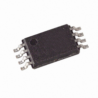
T48C862M-R4-TNS Atmel, T48C862M-R4-TNS Datasheet - Page 38

T48C862M-R4-TNS
Manufacturer Part Number
T48C862M-R4-TNS
Description
IC MON TIRE PRESS 433MHZ 24-SOIC
Manufacturer
Atmel
Datasheet
1.T48C862M-R4-TNS.pdf
(107 pages)
Specifications of T48C862M-R4-TNS
Frequency
433MHz
Modulation Or Protocol
FM, FSK
Data Rate - Maximum
32 kBaud
Power - Output
10dBm
Current - Transmitting
9.5mA
Data Interface
PCB, Surface Mount
Antenna Connector
PCB, Surface Mount
Memory Size
1KB EEPROM, 1KB RAM
Voltage - Supply
2 V ~ 4 V
Operating Temperature
-40°C ~ 125°C
Package / Case
24-SOIC (0.200", 5.30mm Width)
Lead Free Status / RoHS Status
Contains lead / RoHS non-compliant
Features
-
Applications
-
- Current page: 38 of 107
- Download datasheet (2Mb)
Port 4 Data Register (P4DAT)
Port 4 Control Register (P4CR)
Byte Write
Bi-directional Port 6
38
T48C862-R4 [Preliminary]
P4xM2, P4xM1 – Port 4x Interrupt mode/direction code
Table 12. Port 4 Control Register
The bi-directional Port 6 is a bitwise configurable I/O port and provides the external pins
for the Timer 3. As a normal port, it performs in exactly the same way as bi-directional
Port 6 (see Figure 32 on page 37). Two additional multiplexes allow data and port direc-
tion control to be passed over to other internal module (Timer 3). The I/O pin for T3I line
has an additional mode to generate a Timer 3 interrupt.
All two Port 6 pins can be individually switched by the P6CR register. Figure 32 on page
37 shows the internal interfaces to bi-directional Port 6.
Auxiliary Address: "4"hex
3 2 1 0
x x 1 1
x x 1 0
x x 0 1
x x 0 0
1 1 x x
1 0 x x
0 1 x x
0 0 x x
First write cycle
Second write cycle
Code
P4DAT3
Bit 3
Function
BP40 in input mode
BP40 in output mode
BP40 enable alternate function
(SC for SSI)
BP40 enable alternate function
(falling edge interrupt input for
INT3)
BP41 in input mode
BP41 in output mode
BP41 enable alternate function
(VMI for voltage monitor input)
BP41 enable alternate function
(T2I external clock input for
Timer 2)
First Write Cycle
P4DAT2
Bit 2
P41M2
P43M2
Bit 3
Bit 7
P4DAT1
Bit 1
P41M1
P43M1
Bit 2
Bit 6
P4DAT0
Bit 0
Second Write Cycle
3 2 1 0
x x 1 1
1 0 x x
P40M2
P42M2
x x 1 0
x x 0 x
1 1 x x
0 1 x x
0 0 x x
Code
Bit 1
Bit 5
–
Auxiliary register address: "4"hex
Primary register address: "4"hex
Function
BP42 in input mode
BP42 in output mode
BP42 enable alternate function
(T2O for Timer 2)
BP43 in input mode
BP43 in output mode
BP43 enable alternate function
(SD for SSI)
BP43 enable alternate function
(falling edge interrupt input for
INT3)
–
P40M1
P42M1
Bit 0
Bit 4
Reset value: 1111b
Reset value: 1111b
Reset value: 1111b
4551C–4BMCU–01/04
Related parts for T48C862M-R4-TNS
Image
Part Number
Description
Manufacturer
Datasheet
Request
R

Part Number:
Description:
IC MON TIRE PRESS 315MHZ 24SOIC
Manufacturer:
Atmel
Datasheet:

Part Number:
Description:
IC MON TIRE PRESS 433MHZ 24-SOIC
Manufacturer:
Atmel
Datasheet:

Part Number:
Description:
IC MON TIRE PRESS 315MHZ 24SOIC
Manufacturer:
Atmel
Datasheet:

Part Number:
Description:
DEV KIT FOR AVR/AVR32
Manufacturer:
Atmel
Datasheet:

Part Number:
Description:
INTERVAL AND WIPE/WASH WIPER CONTROL IC WITH DELAY
Manufacturer:
ATMEL Corporation
Datasheet:

Part Number:
Description:
Low-Voltage Voice-Switched IC for Hands-Free Operation
Manufacturer:
ATMEL Corporation
Datasheet:

Part Number:
Description:
MONOLITHIC INTEGRATED FEATUREPHONE CIRCUIT
Manufacturer:
ATMEL Corporation
Datasheet:

Part Number:
Description:
AM-FM Receiver IC U4255BM-M
Manufacturer:
ATMEL Corporation
Datasheet:

Part Number:
Description:
Monolithic Integrated Feature Phone Circuit
Manufacturer:
ATMEL Corporation
Datasheet:

Part Number:
Description:
Multistandard Video-IF and Quasi Parallel Sound Processing
Manufacturer:
ATMEL Corporation
Datasheet:

Part Number:
Description:
High-performance EE PLD
Manufacturer:
ATMEL Corporation
Datasheet:

Part Number:
Description:
8-bit Flash Microcontroller
Manufacturer:
ATMEL Corporation
Datasheet:


