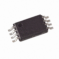
T48C862M-R4-TNS Atmel, T48C862M-R4-TNS Datasheet - Page 52

T48C862M-R4-TNS
Manufacturer Part Number
T48C862M-R4-TNS
Description
IC MON TIRE PRESS 433MHZ 24-SOIC
Manufacturer
Atmel
Datasheet
1.T48C862M-R4-TNS.pdf
(107 pages)
Specifications of T48C862M-R4-TNS
Frequency
433MHz
Modulation Or Protocol
FM, FSK
Data Rate - Maximum
32 kBaud
Power - Output
10dBm
Current - Transmitting
9.5mA
Data Interface
PCB, Surface Mount
Antenna Connector
PCB, Surface Mount
Memory Size
1KB EEPROM, 1KB RAM
Voltage - Supply
2 V ~ 4 V
Operating Temperature
-40°C ~ 125°C
Package / Case
24-SOIC (0.200", 5.30mm Width)
Lead Free Status / RoHS Status
Contains lead / RoHS non-compliant
Features
-
Applications
-
Timer 2 Mode Register 2
(T2M2)
Timer 2 Compare and
Compare Mode Registers
52
T48C862-R4 [Preliminary]
Table 19. Timer 2 Output Select Bits
If one of these output modes is used the T2O alternate function of Port 4 must also be
activated.
Timer 2 has two separate compare registers, T2CO1 for the 4-bit stage and T2CO2 for
the 8-bit stage of Timer 2. The timer compares the contents of the compare register cur-
rent counter value and if it matches it generates an output signal. Dependent on the
timer mode, this signal is used to generate a timer interrupt, to toggle the output flip-flop
as SSI clock or as a clock for the next counter stage.
In the 12-bit timer mode, T2CO1 contains bits 0 to 3 and T2CO2 bits 4 to 11 of the 12-bit
compare value. In all other modes, the two compare registers work independently as a
4- and 8-bit compare register.
When assigned to the compare register a compare event will be suppressed.
Output Mode
T2TOP
T2OS2
T2OS1
T2OS0
T2TOP
Bit 3
1
2
3
4
5
6
7
8
T2OS2
T imer 2 T oggle O utput P reset
This bit allows the programmer to preset the Timer 2 output T2O.
T2TOP = 0, resets the toggle outputs with the write cycle (M2 = 0)
T2TOP = 1, sets toggle outputs with the write cycle (M2 = 1)
Note: If T2R = 1, no output preset is possible
T imer 2 O utput S elect bit 2
T imer 2 O utput S elect bit 1
T imer 2 O utput S elect bit 0
Bit 2
T2OS2
1
1
1
1
0
0
0
0
T2OS1
Bit 1
T2OS1
1
1
0
0
1
1
0
0
T2OS0
T2OS0
Bit 0
1
0
1
0
1
0
1
0
Clock Output (POUT)
Toggle mode: a Timer 2 compare match
toggles the output flip-flop (M2) -> T2O
Duty cycle burst generator 1: the DCG output
signal (DCG0) is given to the output and
gated by the output flip-flop (M2)
Duty cycle burst generator 2: the DCG output
signal (DCGO) is given to the output and
gated by the SSI internal data output (SO)
Biphase modulator: Timer 2 modulates the
SSI internal data output (SO) to Biphase
code
Manchester modulator: Timer 2 modulates
the SSI internal data output (SO) to
Manchester code
SSI output: T2O is used directly as SSI
internal data output (SO)
PWM mode: an 8/12-bit PWM mode
Not allowed
Address: "7"hex - Subaddress: "2"hex
Reset value: 1111b
4551C–4BMCU–01/04


