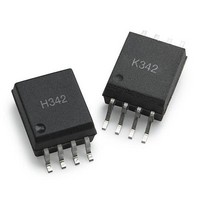
ACPL-K342-060E Avago Technologies US Inc., ACPL-K342-060E Datasheet - Page 15

ACPL-K342-060E
Manufacturer Part Number
ACPL-K342-060E
Description
Logic Output Optocouplers Optocoupler
Manufacturer
Avago Technologies US Inc.
Series
-r
Type
Gate Driver, Miller Clampr
Datasheet
1.ACPL-K342-000E.pdf
(19 pages)
Specifications of ACPL-K342-060E
Fall Time
18 ns
Rise Time
22 ns
Maximum Propagation Delay Time
0.35 us
Maximum Forward Diode Voltage
1.95 V
Minimum Forward Diode Voltage
1.2 V
Maximum Reverse Diode Voltage
5 V
Maximum Continuous Output Current
2.5 A
Maximum Power Dissipation
255 mW
Maximum Operating Temperature
+ 105 C
Minimum Operating Temperature
- 40 C
Package / Case
SOIC-8
No. Of Channels
1
Isolation Voltage
5kV
Optocoupler Output Type
Gate Drive
Input Current
230mA
Output Voltage
30V
Opto Case Style
SOIC
No. Of Pins
8
Peak Reflow Compatible (260 C)
Yes
Rohs Compliant
Yes
Voltage - Isolation
5000Vrms
Input Type
DC
Voltage - Supply
15 V ~ 30 V
Operating Temperature
-40°C ~ 105°C
Mounting Type
Surface Mount
Leaded Process Compatible
Yes
Lead Free Status / RoHS Status
Lead free / RoHS Compliant
Figure 33. Recommended application circuit with split resistors LED drive and active Miller Clamp.
Active Miller Clamp
A Miller clamp allows the control of the Miller current
during a high dV/dt situation. And it can also eliminate
the use of a negative supply voltage by quickly discharg-
ing the large gate capacitance of IGBT to low level without
affecting the IGBT turn-off characteristics. During turn-off,
the gate voltage is monitored and the clamp output is
activated when gate voltage goes below 2.3V (relative to
V
up to 2.5 A. The clamp is disabled when the LED input is
triggered again.
AN5314 application note describes how the clamp reduces
the parasitic turn-on effect due to the Miller capacitor and
at the same time eliminates the need of a negative power
supply.
The Miller pin should be connected to V
Figure 34. Typical gate driver with output stage in darlington configuration
Figure 35. ACPL-H342 with NMOS and PMOS output stage for Rail-to-Rail output voltage
15
CATHODE
CATHODE
EE
ANODE
ANODE
). The clamp voltage is V
NC
NC
NC
NC
+
+
_
_
1
2
3
4
1
2
3
4
R
R
1
2
3
4
ANODE
NC
CATHODE
NC
OL
+2.5V typ for a Miller current
9
V
&/$03
CLAMP
EE
when not in use.
V
CLAMP
V
V
V
V
OUT
8
7
6
5
CC
EE
EE
8
7
6
5
V
V
8
7
6
5
CC
V
OUT
V
V
V
CC
OUT
CLAMP
EE
R
PULL-DOWN
1μF
R
G
Rail-to-Rail Output
Figure 34 shows a typical gate driver’s high current
output stage with 3 bipolar transistors in darlington con-
figuration. During the output high transition, the output
voltage rises rapidly to within 3 diode drops of V
ensure the V
V
to beyond V
to limit the output voltage to V
R
to sink a static current while the output is high.
ACPL-H342 uses a power NMOS follower stage to deliver
the initial large current and a smaller PMOS to pull it to V
to achieve Rail-to-Rail output voltage as shown in Figure
35. This ensures that the IGBT’s gate voltage is driven to
the optimum intended level with no power loss across
IGBT even when an unstable power supply is used.
PULL-DOWN
CE(ON)
R
G
voltage. The level of V
+
+
_
_
V
between the output and V
CC
CC
OUT
=18V
+3(V
is at V
Q1
Q2
BE
) to account for the diode drops. And
CC
in order to achieve IGBT rated
CC
will be need to be raised
CC
, a pull-down resistor,
EE
is recommended
V
V
+
+
+
-
-
CE
CE
+ HVDC
3-PHASE
-HVDC
AC
CC
. To
CC


