ACPL-K342-060E Avago Technologies US Inc., ACPL-K342-060E Datasheet - Page 5
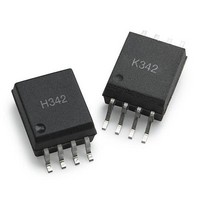
ACPL-K342-060E
Manufacturer Part Number
ACPL-K342-060E
Description
Logic Output Optocouplers Optocoupler
Manufacturer
Avago Technologies US Inc.
Series
-r
Type
Gate Driver, Miller Clampr
Datasheet
1.ACPL-K342-000E.pdf
(19 pages)
Specifications of ACPL-K342-060E
Fall Time
18 ns
Rise Time
22 ns
Maximum Propagation Delay Time
0.35 us
Maximum Forward Diode Voltage
1.95 V
Minimum Forward Diode Voltage
1.2 V
Maximum Reverse Diode Voltage
5 V
Maximum Continuous Output Current
2.5 A
Maximum Power Dissipation
255 mW
Maximum Operating Temperature
+ 105 C
Minimum Operating Temperature
- 40 C
Package / Case
SOIC-8
No. Of Channels
1
Isolation Voltage
5kV
Optocoupler Output Type
Gate Drive
Input Current
230mA
Output Voltage
30V
Opto Case Style
SOIC
No. Of Pins
8
Peak Reflow Compatible (260 C)
Yes
Rohs Compliant
Yes
Voltage - Isolation
5000Vrms
Input Type
DC
Voltage - Supply
15 V ~ 30 V
Operating Temperature
-40°C ~ 105°C
Mounting Type
Surface Mount
Leaded Process Compatible
Yes
Lead Free Status / RoHS Status
Lead free / RoHS Compliant


Table 2. Insulation and Safety Related Specifications
Notes:
1. All Avago data sheets report the creepage and clearance inherent to the optocoupler component itself. These dimensions are needed as a
Table 3. Absolute Maximum Ratings
Table 4. Recommended Operating Conditions
5
Parameter
Minimum External Air Gap
(Clearance)
Minimum External Tracking
(Creepage)
Minimum Internal Plastic Gap
(Internal Clearance)
Tracking Resistance
(Comparative Tracking Index)
Isolation Group
Parameter
Storage Temperature
Operating Temperature
Output IC Junction Temperature
Average Input Current
Peak Transient Input Current
(<1 Ps pulse width, 300pps)
Reverse Input Voltage
“High” Peak Output Current
“Low” Peak Output Current
Peak Clamp Sink Current
Total Output Supply Voltage
Input Current (Rise/Fall Time)
Output Voltage
Output IC Power Dissipation
Total Power Dissipation
Lead Solder Temperature
Parameter
Operating Temperature
Output Supply Voltage
Input Current (ON)
Input Voltage (OFF)
starting point for the equipment designer when determining the circuit insulation requirements. However, once mounted on a printed circuit
board, minimum creepage and clearance requirements must be met as specified for individual equipment standards. For creepage, the shortest
distance path along the surface of a printed circuit board between the solder fillets of the input and output leads must be considered. There are
recommended techniques such as grooves and ribs which may be used on a printed circuit board to achieve desired creepage and clearances.
Creepage and clearance distances will also change depending on factors such as pollution degree and insulation level.
Symbol
L(101)
L(102)
CTI
ACPL-H342
7.0
8.0
0.08
> 175
IIIa
Symbol
T
T
T
I
I
V
I
I
I
(V
t
V
P
P
260°C for 10 sec., 1.6 mm below seating plane
Symbol
T
(V
I
V
F(AVG)
F(TRAN)
OH(PEAK)
OL(PEAK)
CLAMP
F(ON)
r(IN)
A
J
A
S
R
O(PEAK)
O
T
F(OFF)
CC
CC
/ t
- V
- V
f(IN)
EE
EE
)
)
ACPL-K342
8.0
8.0
0.08
> 175
IIIa
Min.
-55
-40
0
-0.5
Min.
- 40
15
7
- 3.6
Units
mm
mm
mm
V
Conditions
Measured from input terminals to output
terminals, shortest distance through air.
Measured from input terminals to output
terminals, shortest distance path along body.
Through insulation distance conductor to
conductor, usually the straight line distance
thickness between the emitter and detector.
DIN IEC 112/VDE 0303 Part 1
Material Group (DIN VDE 0110, 1/89, Table 1)
Max.
125
105
125
25
1
5
2.5
2.5
2.5
35
500
V
210
255
Max.
105
30
16
0.8
CC
Units
°C
°C
°C
mA
A
V
A
A
A
V
ns
V
mW
mW
Units
°C
V
mA
V
Note
1
2
2
2
3
4
Note
Related parts for ACPL-K342-060E
Image
Part Number
Description
Manufacturer
Datasheet
Request
R

Part Number:
Description:
ISOLATOR 5KVRMS 1CH GATE 8SOIC
Manufacturer:
Avago Technologies US Inc.
Datasheet:

Part Number:
Description:
Plastic Optocoupler, LF+T/R
Manufacturer:
Avago Technologies US Inc.
Datasheet:
Part Number:
Description:
Plastic Optocoupler, LF+T/R
Manufacturer:
Avago Technologies US Inc.
Datasheet:

Part Number:
Description:
OPTOCOUPLER GATE DRV 2A 16-SOIC
Manufacturer:
Avago Technologies US Inc.
Datasheet:
Part Number:
Description:
OPTOCOUPLER 2CH 2.5A 16-SOIC
Manufacturer:
Avago Technologies US Inc.
Datasheet:

Part Number:
Description:
OPTOCOUPLER GATE DRV 0.4A 16SOIC
Manufacturer:
Avago Technologies US Inc.
Datasheet:

Part Number:
Description:
OPTOCOUPLER 2.0A 250KHZ 8-DIP
Manufacturer:
Avago Technologies US Inc.
Datasheet:

Part Number:
Description:
OPTOCOUPLER 2.0A 250KHZ GW 8-SMD
Manufacturer:
Avago Technologies US Inc.
Datasheet:

Part Number:
Description:
OPTOCOUPLER 2CH 15MBD 3.3V 8SOIC
Manufacturer:
Avago Technologies US Inc.
Datasheet:
Part Number:
Description:
OPTOCOUPLER DARL-OUT 8-DIP
Manufacturer:
Avago Technologies US Inc.
Datasheet:
Part Number:
Description:
OPTOCOUPLER IGBT DRIVE 0.4A 8DIP
Manufacturer:
Avago Technologies US Inc.
Datasheet:
Part Number:
Description:
OPTOCOUPLER DARL-OUT 8-DIP
Manufacturer:
Avago Technologies US Inc.
Datasheet:

Part Number:
Description:
OPTOCOUPLER 1CH 1MBS 8-SMD GW
Manufacturer:
Avago Technologies US Inc.
Datasheet:
Part Number:
Description:
OPTOCOUPLER GATE DRIVER 8-DIP
Manufacturer:
Avago Technologies US Inc.
Datasheet:

Part Number:
Description:
OPTOCOUPLER GATE DRIVER 8-SMD
Manufacturer:
Avago Technologies US Inc.
Datasheet: