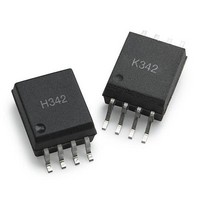
ACPL-K342-060E Avago Technologies US Inc., ACPL-K342-060E Datasheet - Page 7

ACPL-K342-060E
Manufacturer Part Number
ACPL-K342-060E
Description
Logic Output Optocouplers Optocoupler
Manufacturer
Avago Technologies US Inc.
Series
-r
Type
Gate Driver, Miller Clampr
Datasheet
1.ACPL-K342-000E.pdf
(19 pages)
Specifications of ACPL-K342-060E
Fall Time
18 ns
Rise Time
22 ns
Maximum Propagation Delay Time
0.35 us
Maximum Forward Diode Voltage
1.95 V
Minimum Forward Diode Voltage
1.2 V
Maximum Reverse Diode Voltage
5 V
Maximum Continuous Output Current
2.5 A
Maximum Power Dissipation
255 mW
Maximum Operating Temperature
+ 105 C
Minimum Operating Temperature
- 40 C
Package / Case
SOIC-8
No. Of Channels
1
Isolation Voltage
5kV
Optocoupler Output Type
Gate Drive
Input Current
230mA
Output Voltage
30V
Opto Case Style
SOIC
No. Of Pins
8
Peak Reflow Compatible (260 C)
Yes
Rohs Compliant
Yes
Voltage - Isolation
5000Vrms
Input Type
DC
Voltage - Supply
15 V ~ 30 V
Operating Temperature
-40°C ~ 105°C
Mounting Type
Surface Mount
Leaded Process Compatible
Yes
Lead Free Status / RoHS Status
Lead free / RoHS Compliant
Table 6. Switching Specifications (AC)
Unless otherwise noted, all typical values are at T
fications are at Recommended Operating Conditions (T
15 to 30 V, V
Table 7. Package Characteristics
Unless otherwise noted, all typical values are at T
Operating Conditions.
*
Notes:
1. Derate linearly above 70°C free-air temperature at a rate of 0.3 mA/°C.
2. Maximum pulse width = 10Ps
3. Derate linearly above 85°C free-air temperature at a rate of 5.5 mW/°C.
4. Derate linearly above 85°C free-air temperature at a rate of 6.3 mW/°C. The maximum LED junction temperature should not exceed 125°C.
5. Maximum pulse width = 50 μs.
6. In this test V
7. Maximum pulse width = 1 ms.
8. In accordance with UL1577, each optocoupler is proof tested by applying an insulation test voltage t4500 Vrms for 1 second (leakage detection
9. In accordance with UL1577, each optocoupler is proof tested by applying an insulation test voltage t6000 Vrms for 1 second (leakage detection
10. Device considered a two-terminal device: pins 1, 2, 3, and 4 shorted together and pins 5, 6, 7, and 8 shorted together.
11. The difference between t
12. Pins 2 and 4 need to be connected to LED common.
13. Common mode transient immunity in the high state is the maximum tolerable dV
14. Common mode transient immunity in a low state is the maximum tolerable dV
15. This load condition approximates the gate load of a 1200V/150A IGBT.
7
Parameter
Propagation Delay Time to
High Output Level
Propagation Delay Time to
Low Output Level
Propagation Delay Difference
Between Any Two Parts
Rise Time
Fall Time
Output High Level Common
Mode Transient Immunity
Output Low Level Common
Mode Transient Immunity
Parameter
Input-Output Momentary
Withstand Voltage*
Input-Output Resistance
Input-Output Capacitance
LED-to-Ambient Thermal
Resistance
LED-to-Detector Thermal
Resistance
Detector-to-Ambient
Thermal Resistance
The Input-Output Momentary Withstand Voltage is a dielectric voltage rating that should not be interpreted as an input-output continuous
voltage rating. For the continuous voltage rating, refer to your equipment level safety specification or Avago Technologies Application Note 1074
entitled “Optocoupler Input-Output Endurance Voltage. ”
current limit, I
current limit, I
will remain in the high state (i.e., V
will remain in a low state (i.e., V
EE
OH
I-O
I-O
= Ground).
is measured with a dc load current. When driving capacitive loads V
d5 PA).
d5 PA).
PHL
and t
O
Symbol
V
R
C
R
R
R
< 1.0 V).
ISO
I-O
11
12
22
I-O
PLH
O
, R
> 15.0 V).
Symbol
t
t
PDD
(t
t
t
|CM
|CM
between any two ACPL-H342 parts under the same test condition.
PLH
PHL
R
F
21
PHL
H
L
|
- t
|
Device
ACPL-H342
ACPL-K342
PLH
)
Min.
0.100
0.050
-0.010
40
25
40
25
A
A
= 25°C, V
= 25°C; all Minimum/Maximum specifications are at Recommended
Min.
3750
5000
311
111
168
Typ.
0.260
0.145
-0.100
22
18
50
35
50
35
A
= -40 to 105°C, I
Typ.
>50
0.2
CC
- V
Max.
0.350
0.250
-0.200
12
EE
CM
= 30 V, V
Max.
CM
/dt of the common mode pulse, V
OH
/dt of the common mode pulse, V
will approach V
Units
Ps
Ps
Ps
ns
ns
kV/Ps
kV/Ps
F(ON)
Units
V
V
:
pF
°C/W
EE
RMS
RMS
= 7 to 16 mA, V
= Ground; all Minimum/Maximum speci-
Test Conditions
R
C
f = 20 kHz ,
Duty Cycle = 50%,
I
V
V
T
V
V with split resistors
T
V
V without split resistors
T
V
V with split resistors,
T
V
V without split resistors
F
A
A
A
A
g
g
CC
CC
CC
CC
CC
CC
= 7 mA to 16 mA,
Test Conditions
RH < 50%,
t = 1 min., T
RH < 50%,
t = 1 min., T
V
f =1 MHz
Thermal Model in
Application Notes
Below
= 25°C, I
= 25°C, I
= 25°C, V
= 25°C, V
= 10:,
= 25 nF,
CC
I-O
= 15 V to 30V
= 30V
= 30 V, V
= 30 V, V
= 30 V, V
= 30 V, V
as I
= 500 V
OH
F
F
approaches zero amps.
F
F
= 10 mA,
CM
= 10 mA,
CM
CM
CM
= 0 V,
= 0 V,
F(OFF)
A
A
DC
= 25°C
= 25°C
= 1500
= 1000
= 1500
= 1000
CM
CM
, to assure that the output
, to assure that the output
= -3.6 to 0.8 V, V
Fig.
17, 18,
19, 20,
21, 31
39, 40
31
32
32
Fig.
Note
15
11
12, 13
12, 14
Note
8,10
9,10
10
CC
=


